Program
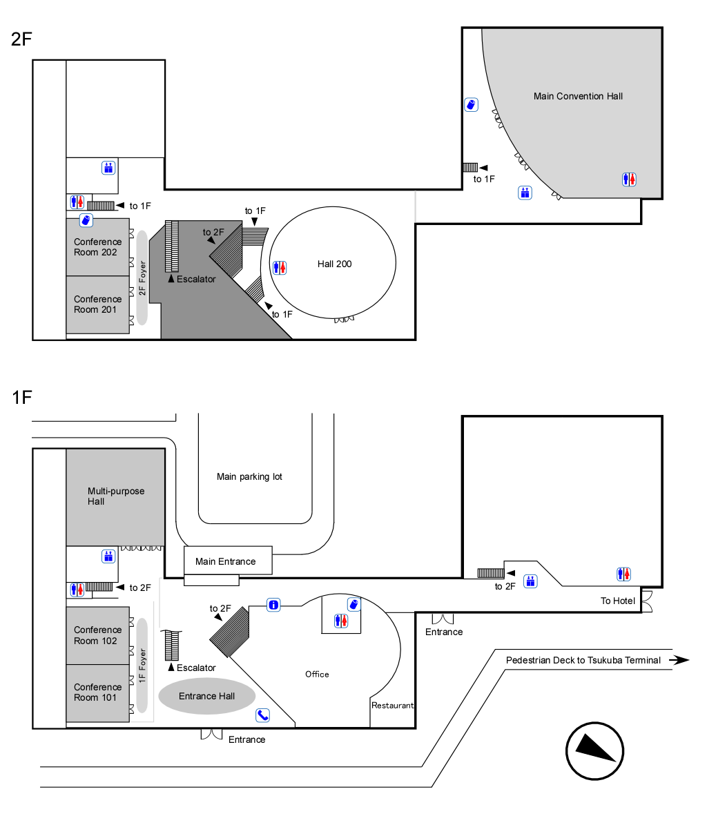
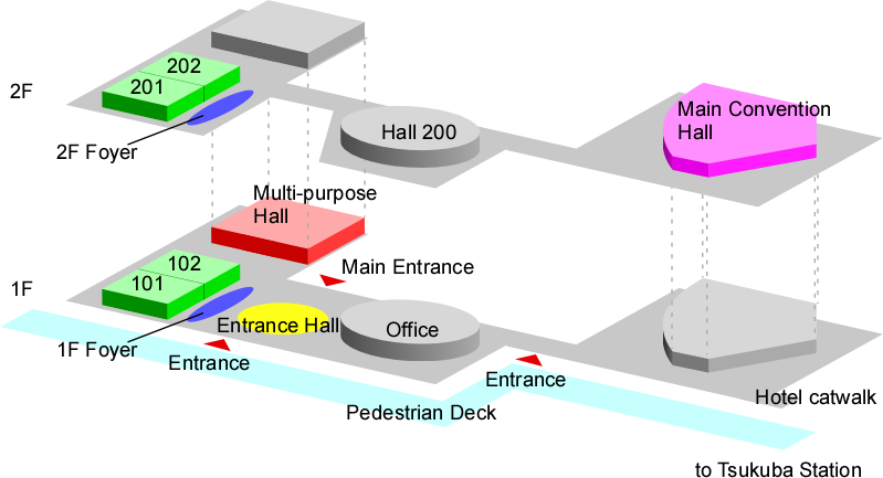
Floor Plan
Conference Overview
- Welcome reception (Nov 4, 17:00, Restaurant ESPOIR)
- On the first day, Nov 4, registration and welcome reception are held. No scientific program is scheduled. Welcome reception starts at 17:00 in Restaurant ESPOIR. It is for free. No reservation is required.
- Oral presentations (Room 101, 102, 201, 202)
- The oral presentations are scheduled in four parallel sessions in room 101, 102, 201 and 202 from Nov 5 to Nov 8.
An invited talks is for 30 min and a contributed talk is for 15 min, including 5 min discussion.
- Poster presentations (Multi-purpose Hall)
- The poster presentations are scheduled in three independent sessions in Multi-purpose Hall on Nov 5, Nov 7 and Nov 8.
- Plenary session (Nov 5, 9:45, Main Convention Hall)
- Plenary session on Nov 5 includes three special talks by Prof. Guy Le Lay from Aix-Marseille University, France, Prof. Toshio Ando from Kanazawa University, Japan and Prof. Seizo Morita from Osaka University, Japan.
- Dr. Heinrich Rohrer Memorial Session (Nov 6, 16:00, Main Convention Hall)
~~ Impact of STM for Future Science and Technology ~~
Dr. Heinrich Rohrer, founding father of nanoscience and nanotechnology, passed away on May 16 of this year.
In 1981, he invented scanning tunneling microscopy (STM) with Dr. Gerd Binnig, which revolutionized surface
science community and paved the way for atomically-controlled nanoworld. In 1986 the two were awarded the Nobel
prize in Physics.
The memorial session on Nov 6, featuring speakers as follows, is intended to discuss the impact of STM for
future science and technology.
- Young Kuk (Seoul National University, Korea)
- Masakazu Aono (National Institute for Materials Science, Japan)
- Tomihiro Hashizume (Hitachi, Ltd., Japan)
- Guy Le Lay (Aix-Marseille University, France)
- Robert. J. Hamers (University of Wisconsin-Madison, USA)
- Kunio Takayanagi (Tokyo Institute of Technology, Japan)
- Nanoscience Prize (Nov 7, 16:15, Main Convention Hall)
- Nanoscience Prize Ceremony is held on Nov 7. There is an award lecture by the prize winner, Dr. Masakazu Aono from National Institute for Materials Science, Japan.
- Banquet (Nov 6, 18:00, Entrance Hall)
The banquet is held on Nov 6 from 18:00 in Entrance Hall. Since the banquet fee is not included in the registration fee, you and possible accompanying person need to register and pay the fee for attendance. It is for free for accompanying person under 6 years old.
At the banquet, Best Poster Awards are presented.
- Excursion (Nov 8, 14:15, City tour to JAXA)
-
The conference excursion on Nov 8 brings you to JAXA, Japan Aerospace Exploration Agency. The participants are requested to gather at the Main Entrance immediately after the closing. It is for free. No need for reservation. There are 90 seats in two buses.
At JAXA, Japanese space carriers, rocket engines, space satellites and Kibou that is Japanese module of the International Space Station (ISS) are on permanent exhibit. There is also a special exhibition featuring some seasonal or up-to-date theme.
One of the two buses departs JAXA to Tsukuba Terminal at 15:25 so that the participants can board the airport bus bound for Narita at 15:50. If you are going to catch this service, bring your luggage with you to the closing ceremony because there is no time to pick up your luggage from the cloak before the departure.
The other bus stops at the conference center before arriving at the Tsukuba Terminal at ~15:50.
- Exhibition (1F Foyer and 2F Foyer)
- A scientific exhibition, including instruments for surface science and nanotechnology, vacuum instruments, surface and interface analysis services, and science books will be held during the conference from Nov 5, 12:00 to Nov. 8, 12:00 at 1F Foyer and 2F Foyer.
- Lunch
- Except for the last day's special lunch, lunch is not served by the conference.
- Luncheon Seminars
- Luncheon seminars by Renishaw KK and Shimazu Corporation are scheduled during the break for lunch, 12:15 – 13:15 in Room 101. All the participants of the conference will be invited for Luncheon seminar. You can take a lunch box free at the seminar room.
Nov 6, "Renishaw Raman-AFM/TERS solutions" by Renishaw KK.
Nov 7, "Cutting Edge Scanning Probe Microscopy" by Shimadzu Corp.
Daily Schedule
Oral Program: November 5 (Tue)
5aH-1 (Plenary)Atom-thin novel 2D materials beyond graphene
G. Le Lay1
1Aix-Marseille University, France
5aH-2 (Plenary)High-speed Atomic Force Microscopy Filming Dynamic Biomolecular Processes
T. Ando1
1Kanazawa University, Japan
5aH-3 (Plenary)Frontiers of Atomically Resolved Force Microscopy at Room Temperature
S. Morita 1
1Osaka University, Japan
5pA1-1 (Invited)Mechanical and electrical properties of atomically defined contacts
P. Grütter1
1McGill University, Canada
5pA1-3Charge Ordered Insulator phase on α-Sn/Ge(111).
I. Palacio1, A. Tejeda1,2, Y. Otshubo1, A. Taleb-Ibrahimi1, E.G. Michel3 and A. Mascaraque4
1Synchrotron SOLEIL, France, 2Institut Jean Lamour, France, 3Univ. Autónoma Madrid, Spain, 4Univ. Complutense Madrid, Spain
5pA1-4Kondo resonance observation of a organic radical molecule
J. Liu1 and T. Komeda2
1Tohoku University, Japan, 2Tohoku University, Japan
5pA1-5Exploring Rashba Spin-Split Surface States on Semiconductors
T. Aruga1, S. Hatta1, K. Yaji1,2 and Y. Ohtsubo1,3
1Kyoto University, Japan, 2University of Tokyo, Japan, 3Synchrotron SOLEIL, France
5pA1-6Large Spin Splitting of Surface-State Bands of Au/Si(111) Surface
L.V. Bondarenko1,2, D.V. Gruznev1,2, A.A. Yakovlev1, A.Y. Tupchaya1, O. Vilkov3, D.V. Vyalikh3,4, S.V. Eremeev5,6, E.V. Chulkov7,8, A.V. Zotov1,2,9 and A.A. Saranin1,2
1IACP, Vladivostok, Russia, 2FEFU, Vladivostok, Russia, 3St.Petersburg State Univ., Russia, 4ISSP, Dresden Univ. of Technol., Germany, 5ISPMS, Tomsk, Russia, 6TSU, Tomsk, Russia, 7DIPC, San Sebastian, Spain, 8UPV/EHU, San Sebastian, Spain, 9VSUES, Vladivostok, Russia
5pB1-1 (Invited)Self-Assembly of C60 Fullerenes on Metal/Silicon Reconstructions
A.V. Zotov1,2,3, A.V. Matetskiy1,2, L.V. Bondarenko1,2, D.V. Gruznev1,2, A.A. Saranin1,2, J.P. Chou4, C.M. Wei4, M.Y. Lai4 and Y.L. Wang4
1Institute of Automation and Control Processes, Russian Federation, 2Far Eastern Federal University, Russian Federation, 3Vladivostok State University of Economics and Service, Russian Federation, 4Institute of Automic and Molecular Sciences, Taiwan
5pB1-3Point Defect Characterization in InGaN by Using Monoenergetic Positron Beams
A. Uedono1, T. Watanabe1, S. Kimura1, Y. Zhang1, M. Lozac'h1, L. Sang2, S. Ishibashi3, N. Oshima3, R. Suzuki3 and M. Sumiya2
1University of Tsukuba, Japan, 2NIMS, Japan, 3AIST, Japan
5pB1-5Developing of a TiO2 Nanostructure Towards Efficient Water Splitting
Y. Pihosh1, K. Mawatari1, I. Turkevych2, M. Tosa2 and T. Kitamori1
1The University of Tokyo, JAPAN, 2National Institute for Materials Science, JAPAN
5pB1-6Formation of ultrahigh density Fe-based nanodots on Si substrates by controlling Ge nuclei on ultrathin SiO2 film
R. Sugimoto1, Y. Nakamura1,2, H. Matsui1, J. Kikukawa1 and A. Sakai1
1Osaka Univeristy, Japan, 2PRESTO-JST, Japan
5pC1-1 (Invited)Synchrotron X-ray scanning tunneling microscopy
V. Rose1
1Argonne National Laboratory, USA
5pC1-3Atomistic Simulation of AFM Indentation of Gold Nanoclusters and Nanorods
B. Reischl1, K. Nordlund1, H. Husu2, V. Korpelainen2 and A. Lassila2
1University of Helsinki, Finland, 2MIKES, Finland
5pC1-4Three-dimensional impurity distribution at sigma-3{111} grain boundaries in Si by atom probe tomography combined with transmission electron microscopy
Y. Ohno1, K. Inoue1, I. Yonenaga1, N. Ebisawa2, H. Takamizawa2, Y. Shimizu2, K. Inoue2, Y. Nagai2, H. Yoshida3, S. Takeda3, Y. Tokumoto and K. Kutsukake
1IMR, Tohoku University, Sendai 980-8577, Japan, 2The Oarai Center, IMR, Tohoku University, Ibaraki 311-1313, Japan, 3ISIR, Osaka University, Osaka 567-0047, Japan
5pC1-5Structure of SiC grown Graphene probed by fast atom diffraction
M. Debiossac1, H. Khemliche1, P. Lunca-Popa1, A. Momeni1,2, A. Mayne1, A. Zugarramurdi1 and P. Roncin1
1ISMO, Université Paris Sud, Orsay, France, 2LERMA, Université de Cergy-Pontoise, France
5pC1-6STEM Characterisation of Ga(NAs)/Ga(AsBi) Interfaces
N. Knaub1, A. Beyer1, J. Muenzner1, P. Ludewig1, Z. Bushell1,2, W. Stolz1 and K. Volz1
1Philipps-Universität Marburg, Germany, 2University of Surrey, Guildford, UK
5pD1-1 (Invited)The quantum and classical properties of spins on surfaces
A. Heinrich1
1Almaden Research Center, USA
5pD1-3STM-induced Luminescence from Single Phthalocyanine Molecules
H. Imada1, M. Imai2, T.K. Shimizu3, M. Kawai2 and Y. Kim1
1RIKEN, Japan, 2The University of Tokyo, Japan, 3NIMS, Japan
5pD1-4Laser-induced Electron Emission from Tungsten Tip in Strong Field Regime
H. Yanagisawa1
1ETH Zurich, Switzerland
5pD1-5Cathodoluminescence Study of Plasmonic Cavities
N. Yamamoto1
1Physics Dept., Tokyo Institute of Technology, Japan
5pD1-6Nanometers Resolution Chemical Analysis by Tip Enhanced Raman Imaging
C. Chen1,2, N. Hayazawa1 and S. Kawata1,3
1RIKEN, Japan, 2Academia Sinica, Taiwan, 3Osaka Univ., Japan
5pA2-1 (Invited)Nano-Voids and Nano-Objects at Semiconductor Surface and Sub-Surface
P. Soukiassian1
1Universite de Paris-Sud, France
5pA2-3STM Studies of an Ultrathin Silica Film Epitaxially Formed on the C-Face of 4H-SiC Basal Planes
H. Tochihara1, T. Shirasawa2, T. Suzuki1, T. Miyamachi2, T. Kajiwara3, K. Yagyu1, S. Yoshizawa2, T. Takahashi2, F. Komori2 and S. Tanaka3
1Fukuoka Univ., Japan, 2Univ. of Tokyo, Japan, 3Kyushu Univ., Japan
5pA2-4Spin reorientation transitions of Ni/Cu(100) in an electrolytic condition
J.S. Tsay1, C.L. Lin1, A.W. Wu1, Y.C. Wang1 and Y.C. Tseng1
1National Taiwan Normal University, Taiwan
5pA2-5 (Invited)Optical and Electrical Manipulation in STM of a Single Bi-Stable Si-Atom in GaAs
P. M. Koenraad1
1Eindhoven University of Technology, Netherlands
5pA2-7Structural Defects & Titanium Self-Doping in TiSe2:
Scanning Tunneling Microscopy/Spectroscopy Study and Ab-Initio Calculations
C. Didiot1, B. Hildebrand1, G. Monney1, E.F. Schwier2, A.M. Novello3, A. Scarfato3, A. Ubaldini3, H. Berger4, C. Renner3, D. Bowler5 and P. Aebi Affiliation N°1
1Department of Physics and Fribourg Center for Nanomaterials, Switzerland, 2HiSOR, Japan, 3University of Geneva, Switzerland, 4EPF Lausanne, Switzerland, 5London Center for Nanotechnology, England
5pA2-8Real-time Scanning Tunneling Microscopy Observation of Ni Ion Irradiation Process on Si(111) Surfaces
K. Mura1, T. Kamioka2, T. Kitani1, K. Imazu1 and T. Watanabe1
1Waseda Univ., Japan, 2Tyota Technol. Inst., Japan
5pB2-1 (Invited)STM observation of edge states of 1D and 2D topological insulators
H. W. Yoem1
1POSTECH, Korea
5pB2-4Low Dimensional Electronic States in Reconstructed Au(100)
A. Mascaraque1, S. Bengio2, V. Navarro1, M.A. Gonzalez-Barrio1, R. Cortes1, I. Vobornik3 and E.G. Michel2
1Universidad Complutense de Madrid, Spain, 2Universidad Autónoma de Madrid, Spain, 3IOM-CNR Trieste, Italy
5pC2-1 (Invited)On-Surface Chemistry and Magneto-chemistry: A New Toolbox to Assemble Molecules and Operate their Electron and Spin States
T. A. Jung1
1Paul Scherrer Institute, Switzerland
5pC2-3Photochromism of Diarylethene at the nanoscale
A. Arramel1, T.C. Pijper2, T. Kudernac2, N. Katsonis2, M. van der Maas3, B.L. Feringa2 and B.J. van Wees1
1Zernike Institute of Advanced Materials, Netherlands, 2Stratingh Institute for Chemistry, Netherlands, 3Institute for Molecules and Materials, Netherlands
5pC2-4Controllable intermolecular and molecule-substrate interactions in molecular self-assembled monolayer under laser excitation
Y. Du1, X. Xun1, K.W. See1, G. Peleckis1, X.L. Wang1 and S.X. Dou1
1ISEM, AIIM, University of Wollongong, Wollongong, NSW 2500, Australia
5pD2-1 (Invited)Microscopic Understanding of Spin Filtering at Metal-Organic Interfaces
M. Aeschlimann1
1University of Kaiserslautern, Germany
5pD2-3Adsorption induced spin-state change in MnPc/Pb(111)
E. Minamitani1, Y. Fu1, Q. Xue2 and Y. Kim1
1RIKEN, Japan, 2Depertment of Physics, Tsinghua University, China
5pD2-4Real-space Observation of Superconducting Proximity Effect by Scanning Tunneling Microscopy and Spectroscopy
H. Kim1 and Y. Hasegawa1
1The Institute for Solid State Physics, The University of Tokyo, Japan
5pB2-5 (Invited)Nanostructured Diamond for Renewable Energy and Sustainability
R. J. Hamers1
1University of Wisconsin-Madison, USA
5pB2-7Scanning Probe Microscopy and Spectroscopy of Nanodiamonds
R. Pawlak1, Th. Glatzel1, S. Kawai1, S. Fremy1, L. Schmidlin2, V. Pichot2, D. Spitzer2 and E. Meyer1
1University of Basel, Switzerland, 2Institut Franco-Allemand de Recherches de Saint-Louis, France
5pB2-8Site-specific Measurement of Atomic Dipole Moment Induced Surface Potential on Si(111)-(7×7) by Noncontact Scanning Nonlinear Dielectric Microscopy
K. Yamasue1, M. Abe2, Y. Sugimoto3 and Y. Cho1
1Tohoku Univ., Japan, 2Nagoya Univ., Japan, 3Osaka Univ., Japan
5pB2-9Graphene on Pt(111): Low Temperature Noncontact Atomic Force Microscopy Measurements and First-Principles Calculations
B. delaTorre1, P. Pou1, N. Nicoara1,2, R. Perez1 and J.M. Gomez-Rodriguez1
1Universidad Autonoma de Madrid, Spain, 2Iberian Nanotechnology Laboratory, Portugal
5pC2-5 (Invited)Scanning ion conductance microscopy for imaging biological samples
T. Ushiki1
1Niigata University, Japan
5pC2-7Immunoactivity of IgG Antibody Assembly Investigated by FM-AFM
H. Kominami1, S. Ido1, H. Kimiya2, K. Kobayashi1 and H. Yamada1
1Kyoto Univ., Japan, 2Panasonic Corp., Japan
5pC2-8Electrically Conductive Peptide Networks
R.C.G. Creasey1, Y. Kato1, J. Xu1, Y. Shingaya1 and T. Nakayama1
1National Institute for Materials Science, Japan
5pD2-5 (Invited)Atomic-resolution environmental transmission electron microscopy for quantitative in-situ microscopy in materials science
S. Takeda1
1Osaka University, Japan
5pD2-7Control of Graphene Oxide Film Formation on Surface-Modified Substrates and its Morphological Changes during Reduction
T. Takami1, T. Ito1 and T. Ogino1
1Yokohama National University, Japan
5pD2-8A Novel Phosphate Extended Gate FET Device
W. Chaisriratanakul1, W. Bunjongpru1, S. Porntheeraphat1, W. Jeamsaksiri1, A. Srisuwan1, E. Chaowicharat1, C. Hruanun1 and A. Poyai1
1National Electronics and Computer technology Center, Thailand
Oral Program: November 6 (Wed)
6aA1-1 (Invited)Spin LEGOs – Bottom-up Fabrication of Model Magnetic Systems
A. Khajetoorians1
1University of Hamburg, Germany
6aA1-3A MULTIFUNCTIONAL SINGLE MOLECULAR MEMORY
T. Miyamachi1,2,3, M. Gruber1,4, V. Davesne1,4, E. Beaurepaire4 and W. Wulfhekel1,2
1Karlsruhe Institute of Technology (KIT), Germany, 2DFG-Center for Functional Nanostructures, KIT, Germany, 3ISSP, University of Tokyo, Japan, 4ICPMS, France
6aA1-4Fabrication and Control of Pb-trimer Switch Operable at Room Temperature Using a Combined AFM/STM
E. Inami1, Y. Sugimoto1, M. Abe2 and S. Morita3
1Osaka University, Japan, 2Nagoya University, Japan, 3Osaka University, Japan
6aA1-5Atom manipulation on an insulating surface at room temperature
S. Kawai1, A.S. Foster2, F. Federici Canova3,4, H. Onodera5, S. Kitamura5 and E. Meyer1
1Univrsity of Base, Switzerland, 2Aalto University, Finland, 3Tempere University of Technology, Finland, 4Tohoku University, Japan, 5JEOL Limiter, Japan
6aB1-1 (Invited)Simulation Study on Thermoelectric Properties of Carbon Nanostructures
T. Yamamoto1
1Tokyo University of Science, Japan
6aB1-3AC Response of Carbon Nanotubes with Randomly Distributed Impurities
D. Hirai1, T. Yamamoto2 and S. Watanabe1
1The University of Tokyo, Japan, 2Tokyo University of Science, Japan
6aB1-43D Force Field Spectroscopy Study on Local Reactivity of Single-Walled Carbon Nanotubes with Different Tube Diameters
M. Ashino1,2, S. Adachi2, N. Sasaki3 and R. Wiesendanger1
1Univ. Hamburg, Germany, 2Kanazawa Inst. Tech., Japan, 3Seikei Univ., Japan
6aB1-5Beam Induced Graphitic Carbon Cage Transformation from Sumanene Aggregate
M. Tachi1,2, K. Murakami1,2, H. Sakurai3 and J. Fujita1,2
1University of Tsukuba, Japan, 2Tsukuba Research Center for Interdisciplinary Materials Scienece(TIMS), Japan, 3Institute for Molecular Science, Japan
6aC1-1 (Invited)III-V semiconductor nanowires and their photovoltaic device applications
T. Fukui1
1Hokkaido University, Japan
6aC1-3Shifting and Stretching of Capacitance Curves of Metal/Insulator/AlGaN/GaN Heterostructures by Interface Traps
J. Osvald1
1Institute of Electrical Engineering, Slovak Academy of Sciences, Slovakia
6aC1-4Metal-metal bonidng properties of copper oxide nanoparticles
T. MAEDA1, Y. KOBAYASHI1, Y. YASUDA2 and T. MORITA2
1Ibaraki Univ, Japan, 2Hitachi Research Lab, Japan
6aC1-5Energy-dependent Scattering Phase-Shift of Electrons in 2D Subband States
K. Nagaoka1, S. Yaginuma1 and T. Nakayama1,2
1NIMS, Japan, 2Univ. of Tsukuba, Japan
6aD1-1 (Invited)Gold nanostructures on pure and doped oxide thin films
G. Pacchioni1
1Universit degli Studi Milano-Bicocca, Italy
6aD1-3Decoration of Titanate Nanowires and Nanotubes by Gold Nanoparticles: XPS, LEIS, HRTEM and XRD Characterization
J. Kiss1, P. Pusztai2, L. Ovari2, G. Merza1, A. Oszko1, K. Baan1, A. Erdohelyi1, A. Kukovecz2 and Z. Konya2
1Dept. of Phys. Chem. and Mater. Scie. Univ. of Szeged, Hungary, 2Dept.of Appl. and Environ. Chem. Univ. of Szeged, Hungary
6aD1-4Rotational and Nuclear-Spin State Transition of Hydrogen in Scattering on Electron-Density Controlled SrTiO_3(001) Surfaces
K. Takeyasu1, S. Ogura1 and K. Fukutani1
1The Univ. of Tokyo, Japan
6aA2-1 (Invited)Nanostructured Wide Bandgap Semiconductor Heterostructures for Alternative Device Applications
E.F. DA SILVA JR.1
1UNIVERSIDADE FEDERAL DE PERNAMBUCO, BRAZIL
6aA2-3Stability of Sulfurated InSb Surfaces after Deposition of Dielectric Layers
D. AUREAU1, H. SIK2, J. FLEURY2 and A. ETCHEBERRY1
1Institut Lavoisier, UMR 8180 UVSQ-CNRS, FRANCE, 2Sagem Defense Securite, FRANCE
6aA2-4High-resolution HAADF Studies of GaP/Si-interfaces
A. Beyer1, K. Jandieri1, K. Werner1, A. Stegmüller2, W. Stolz1, R. Tonner2 and K. Volz1
1Faculty of Physic, Philipps-Universität Marburg, Germany, 2Faculty of Chemistry, Philipps-Universität Marburg, Germany
6aA2-5EXAFS study on local structures around Bi atoms in Bi wire-δ-doped Si crystal
K. Murata1,2,3, K. Nitta4, Y. Terada4, T. Uruga4, K. Nittoh2, O. Sakata2 and K. Miki1,2
1University of Tsukuba, Japan, 2National Institute for Materials Science, Japan, 3Japan Society for the Promotion of Science, Japan, 4Japan Synchrotron Radiation Research Institute, Japan
6aB2-1 (Invited)Transport and optoelectronic properties of atomic and molecular junctions
G. Schull1
1IPCMS Strasbourg, France
6aB2-3Tuning the Electric Conductance of Metal Strings via Electrochemical Control
C.-h. Chen1, M.-J. Huang1, H.-C. Lu1, K.-N. Shih1, M.-D. Fu1, I-W.P. Chen1, C.-H. Hsu1, C.-H. Jiang1 and S.-M. Peng1,2
1Natl Taiwan Univ, Taiwan, 2Academia Sinica, Taiwan
6aB2-4Conduction Paths in Tantalum-Oxide-based Resistive Switches: First-Principles Study
B. Xiao1
1Department of Materials Engineering, The University of Tokyo, Tokyo, Japan
6aB2-5Current Rectification in Mono- and Bi-layer Nanographenes with Different Edges
A. Staykov1 and P. Tzenov2
1I2CNER, Kyushu University, Japan, 2Technical University Munich, Germany
6aC2-1 (Invited)Bridging the pressure gap in the surface and interface analysis using electron transparent membranes
A. Kolmakov1
1National Institute of Standards and Technology, USA
6aC2-3High-speed Surface X-ray Diffraction Measurement in a Multi-wavelength Dispersive Mode
T. Shirasawa1, E. Arakawa2, W. Voegeli2, T. Takahashi1 and T. Matsushita3
1Univ. of Tokyo, Japan, 2Tokyo Gakugei Univ., Japan, 3KEK-PF, Japan
6aC2-4MagSAXS: Resonant Magnetic Soft X-ray Small Angle Scattering Setup for Extreme Sample Environment
S. Stanescu1, C. Mocuta1, F. Merlet2 and A. Barbier2
1Synchrotron SOLEIL, France, 2CEA - Saclay, France
6aC2-5Development of an Ionic-liquid Ion Beam Source for Secondary Ion Mass Spectrometry (SIMS)
Y. Fujiwara1 and N. Saito1
1National Institute of Advanced Industrial Science and Technology, Japan
6aD2-1 (Invited)Si-Based New Material for Thin-Film Solar Cells
T. Suemasu1
1University of Tsukuba, Japan
6aD2-3Production and Detection of OH Species by a Highly Concentrated Ozone Gas for Thin Film Processing
T. Miura1, N. Kameda1, M. Kekura1, H. Nonaka2 and K. Nakamura2
1Meidensha Corporation, Japan, 2AIST, Japan
6aD2-4Surface Energy Anisotropy of Clean and Hydrodgen Covered 3C-SiC Surfaces
S.N. Filimonov1, Yu.Yu. Hervieu1, S. Jiao2, S. Sambonsuge2 and M. Suemitsu2
1Tomsk State University, Russia, 2Tohoku University, Japan
6aD2-5Well-ordered Iron Oxide Films on Ag(001)
D. Bruns1, J. Rodewald1, S. Jentsch1, S. Lindemann1 and J. Wollschläger1
1Universität Osnabrück, Germany
6pA1-1 (Invited)Probing solid-liquid interfaces at the atomic scale
A. Foster1
1Aalto University, Finland
6pA1-3Adsorption of Dissolved Gas at a Hydrophobic/Water Interface
I.-S. Hwang1, C.-W. Yang1 and Y.-H. Lu1
1Institute of Physics, Academia Sinica, Taiwan
6pA1-4Preparation and Characterization of ZnO Thin Films grown on Au(111)
L. Pascua1, F. Stavale1, N. Nilius1 and H.-J. Freund1
1Fritz-Haber-Institut of the Max-Planck-Society, Germany
6pB1-1 (Invited)Arrays of Functionalized Nanoparticles for Capturing Bacteria and Monitoring Their Response to Antibiotics via Surface-Enhanced Raman Scattering (SERS)
Y.-L. Wang1
1Academia Sinica, Taiwan & National Taiwan University, Taiwan
6pB1-3Atomic-resolution Imaging of Crystal Growth Process by High-speed FM-AFM
K. Miyata1, H. Asakawa1 and T. Fukuma1,2
1Kanazawa University, Japan, 2ACT-C, Japan Science and Technology Agency, Japan
6pB1-4High-resolution FM-AFM Analysis on Ionic-Liquid/Ionic-Crystal Interfaces
T. Ichii1, M. Negami1 and H. Sugimura1
1Kyoto University, Japan
6pC1-1 (Invited)Electromechanical Properties of Atomic and Molecular Junctions
J. Hihath1
1University of California, Davis, USA
6pC1-3Obtaining detailed information of supramolecular structures by combining high-resolution force microscopy with ab initio calculations
S. Kawai1, A. Sadephi1, X. Feng2, P. Lifen2, R. Pawlak1, T. Glatzel1, A. Willand1, A. Orita2, J. Otera2, S. Goedecker1 and E. Meyer 1
1University of Basel, Switzerland, 2Okayama University of Science, Japan
6pC1-4KPFM Study of Model Donor-Acceptor Self-Assemblies for Organic Photovoltaics
F. Fuchs1, C.J. F. de Vet1, M. Linares2, R. Demadrille1 and B. Grévin1
1CEA CNRS UJF UMR5819 SPrAM Grenoble, France, 2Department of Computational Physics, IFM, Linköping University, Sweden
6pD1-1 (Invited)Single molecular spintronics: spin transport through a single molecule by means of spin-polarized STM
T.K. Yamada1
1Chiba University, Japan
6pD1-3Superparamagnetic Response of Fe-coated W tips in Spin-polarized Scanning Tunneling Microscopy
J.A. Fischer1,2, S. Phark1, M. Corbetta1, D. Sander1 and J. Kirschner1
1Max-Planck-Institute of Microstructure Physics, Germany, 2Universidade Federal de Santa Catarina, Brazil
6pD1-4Theory of spin polarization induced at molecule-metal interfaces
I. Hamada1
1National Institute for Materials Science, Japan
6pA2-1 (Invited)In situ Structural Analyses of Electrochemical Interfaces by EC-FM-AFM
K.-i. Fukui1
1Osaka University, Japan
6pA2-3Structural and electronic properties of TiOx nanoplatelets on Au(111)
P. Carrozzo1, F. Tumino1, C.S. Casari1, M. Passoni1, C.E. Bottani1 and A. Li Bassi1
1Politecnico di Milano, Italy
6pA2-4"Morphological Evolution from a rough to biphase surface of TiO2(100)"
T. Uehara1, M. Yoshihara1 and T. Ogino1
1Yokohama National University, Japan
6pB2-1 (Invited)Individual Molecules Investigated with Atomically Functionalized Tips
L. Gross1
1IBM Research-Zurich, Switzerland
6pB2-3STM Study of Photochromic Diarylethene Adsorbed on Noble Metals
T.K. Shimizu1,2, J. Jung1, H. Imada1 and Y. Kim1
1RIKEN, Japan, 2National Institute for Materials Science, Japan
6pB2-4Stepwise rotation of Pt-porphyrin derivative molecules on a Au(111) surface
P. Mishra1, T. Nakayama1, T. Uchihashi1, T. Ono2, Y. Nakajima2, F. Ozawa2, J. Hill1, W.V. Rossom1, K. Ariga1 and C. Joachim3
1MANA, NIMS, Japan, 2ICR, Kyoto University, Japan, 3CEMES, CNRS, France
6pC2-1 (Invited)The Nuclear Pore Complex: A Paradigm for Molecular Transport Control
R. Lim1
1University of Basel, Switzerland
6pC2-3A novel fabrication technique for suspended plasmonic nanopore sensing devices
J. Junesch1, T. Sannomiya2 and J. Vörös1
1ETH Zurich, Switzerland, 2Tokyo Institute of Technology, Japan
6pC2-4Nanobiodevice for mimicking synaptic connections
K. Sumitomo1, N. Kasai1, Y. Kashimura1, A. Tanaka1, T. Goto1, A. Oshima1, S. Tsukada1 and H. Nakashima1
1NTT Basic Research Laboratories, Japan
6pD2-1Structures and magnetic properties of Co/rubrene/Si(100) films
J.S. Tsay1, C.Y. Hsu1 and C.H.T. Chang1
1National Taiwan Normal University, Taiwan
6pD2-2Scanning tunneling microscopy Investigation of the interfacial electronic properties between YBa2Cu3O7-δ and La0.7Ca0.3MnO3
B. C. Huang1, V. T. Tra2, J. Y. Lin2, Y. P. Chiu1 and Y. H. Chu2
1National Sun Yat-sen University, Taiwan, R.O.C, 2National Chiao Tung University, Taiwan, R,O,C
6pD2-3XMCD Study of Magnetic Proximity Effects in FM(Co, Ni) - AFM(MnF2, NiF2) Heterostructures
N.S. Sokolov1, A.G. Banshchikov1, D.A. Baranov1, V.V. Fedorov1, K.V. Koshmak1,2, L. Pasquali2 and S.M. Suturin1
1Ioffe Physical-Technical Institute, Russia, 2University of Modena & Reggio Emilia, Italy
6pD2-4One-dimensional Non-collinear Spin-ordering in a Fe Nanoisland on Cu(111)
S. Phark1, J. Fischer1, M. Corbetta1, D. Sander1 and J. Kirschner1
1Max-Planck-Institute of Microstructure Physics, Germany
Oral Program: November 7 (Thu)
7aA1-1Single and Multi-Layer Silicene: Growth, Properties and Perspectives
P. Vogt1, A. Resta2, T. Bruhn1,2, P. De Padova3 and G. Le Lay2,3
1TU Berlin, Germany, 2Aix-Marseille University, France, 3CNR-ISM, Italy
7aA1-2The Electronic Structure of Single Layer Silicene on Ag(111)
C.-L. Lin1, R. Arafune2, K. Kawahara1, M. Kanno1, N. Tsukahara1, E. Minamitani3, Y. Kim3, M. Kawai1 and N. Takagi1
1The University of Tokyo, Japan, 2NIMS, Japan, 3RIKEN, Japan
7aA1-3Geometric and Electronic Structure Change of Silicene by interacting with Ag(111) : DFT Analysis
R. Arafune1, C.-L. Lin2, K. Kawahara2, M. Kanno2, N. Tsukahara2, E. Minamitani3, Y. Kim3, M. Kawai3 and N. Takagi3
1NIMS, Japan, 2The University of Tokyo, Japan, 3RIKEN, Japan
7aA1-4Direct View of silicon initial growth on metal surfaces
T. Y. Fu1, Y. C. Chen1 and R. J. Lin1
1National Taiwan Normal University, Taiwan
7aA1-5Total Reflection Positron Diffraction for Surface Structure Analysis
T. Hyodo1, Y. Fukaya2, I. Mochizuki1, M. Maekawa2, K. Wada1 and A. Kawasuso2
1High Energy Accelerator Research Organization (KEK), Japan, 2Japan Atomic Energy Agency, Japan
7aB1-1 (Invited)Ultrafast spin dynamics probed by time-resolved STM
S. Yoshida1, Y. Aizawa1, Z. Wang1, Y. Mera2, E. Matsuyama1, O. Takeuchi1 and H. Shigekawa1
1University of Tsukuba, Japan, 2University of Tokyo, Japan
7aB1-3Spectral broadening in height controlled single GaAs quantum dots formed by droplet epitaxy
N. Ha1,2, T. Mano1, T. Kuroda1,2, J. Bocquel3, P. Koenraad3, Y.L. Chou4, Y.-N. Wu4, S.-J. Cheng4, S. Sanguinetti5, Y. Sakuma1 and K. Sakoda
1NIMS, Japan, 2Kyushu Univ., Japan, 3Eindhoven Univ. Tech.,, Netherlands, 4Nat. Chiao Tung Univ., Taiwan, 5L-NESS and Univ. Milano Bicocca, Italy
7aC1-1 (Invited)Physics of SiC MOS Interface for High-Voltage Power Devices
T. Kimoto1
1Kyoto University, Japan
7aC1-3Interface Dipole Modulation in HfO2/Si structures
N. Miyata1
1AIST, Japan
7aC1-4Temperature Dependence of Strained Si Atoms at SiO2/Si(111) Interface Studied by Real-time X-ray Photoelectron Spectroscopy
J.Y. Tang1, K. Nishimoto1, S. Ogawa1, A. Yoshigoe2, S. Ishidzuka3, D. Watanabe1, Y. Teraoka2 and Y. Takakuwa1
1Tohoku University, Japan, 2Japan Atomic Energy Agency, Japan, 3Nagaoka University of Technology, Japan
7aD1-1 (Invited)Time-Resolved Scanning Tunneling Microscopy Applied to Atomic Spin Arrays
S. Loth1
1Max Planck Institute Hamburg, Germany
7aD1-3Spin-Polarization in Non-Magnetic Resonant Tunneling Diodes
Y. Galvao Gobato1, H.V. Avanço Galeti1, V. Orsi Gordo1 and M. Henini2
1Federal University of São Carlos, Brazil, 2Universtiy of Nottingham, Nottingham
7aD1-4Electrical Conductance through Spin-split Surface States on Pb/Ge(111)
S. Hatta1, T. Noma1, H. Okuyama1 and T. Aruga1
1Graduate School of Science, Kyoto University, Japan
7aD1-5Theoretical and Experimental Study of the Kondo Effect in the Simplest Radical Molecule on Au(111).
S. Modesti1, R. Requist2, P.P. Baruselli2,3, A. Smogunov4, M. Fabrizio2,3 and E. Tosatti2,3,5
1University of Trieste, Italy, 2SISSA, Italy, 3CNR-IOM, Italy, 4DSM-CEA, France, 5ICTP, Italy
7aA2-1 (Invited)Effect of Surface Potential and Ion Structure on Ionic Liquid Lubrication
R. Atkin1
1The University of New Castle, Australia
7aA2-3Potential-Dependent Adsorption/Desorption Behavior of Perfluorosulfonated Ionomer on a Gold and a Platinum Electrode Surface Studied by Electrochemical Quartz Crystal Microbalance and Atomic Force Microscopy
T. Masuda1,2 and K. Uosaki2,3
1Japan Science and Technology Agency, Japan, 2National Institute for Materials Science, Japan, 3Hokkaido University, Japan
7aA2-4First-principles molecular dynamics study of the electric double layer formed on Li-LiBH4 interface
Y. Ando1, T. Ikeshoji1,2 and M. Otani1
1National Institute for Advanced Science and Technology, Japan, 2Tohoku University, Japan
7aA2-5Atomic-Scale Interfacial Band Mapping across Vertically Phased-Separated Polymer/Fullerene Hybrid Solar Cells by Cross-sectional STM
Y. P. Chiu1, M. C. Shih1, B. C. Huang1, C. C. Lin2, S. S. Li2, H. A. Chen2 and C. W. Chen2
1National Sun Yat-sen University, Taiwan, 2National Taiwan University, Taiwan
7aB2-1 (Invited)Graphene Plasmonics: Challenges and Opportunities
F. J. García de Abajo1
1Instituto de Química-Física ""Rocasolano"" - CSIC, Spain
7aB2-3Band gap opening on graphene nanoribbons
A. Tejeda1,2, A. Taleb-Ibrahimi2, J. Hicks3, M.S. Nevius3, F. Wang3, W.A. de Heer3, C. Berger3 and E.H. Conrad3
1Université de Lorraine, France, 2Synchrotron SOLEIL, France, 3GeorgiaTech, USA
7aB2-4Morphological characterization of graphene nanoribbons on SiC.
I. Palacio1, A. Celis1, A. Tejeda1,2, M. Sicot2, E.H. Conrad3, C. Berger3, W. de Heer3, A. Taleb-Ibrahimi1 and D. Malterre2
1Synchrotron SOLEIL, France, 2Institut Jean Lamour, France, 3GeorgiaTech, U.S.A.
7aC2-1 (Invited)The Role of van der Waals Forces in Molecule-Electrode Coupling: Turning around a Molecular Diode
C. A. Nijhuis1
1National Univ. Singapore, Singapore
7aC2-3Investigation of Carrier Behavior in F4TCNQ-Doped P3HT Layer and Its Application to Electrodes of Organic Thin Film Transistors
D. Tadaki1, T. Ma1, J. Zhang1, S. Iino1, Y. Kimura1 and M. Niwano1
1Tohoku University, Japan
7aC2-4Organic Transparent Electrodes Applied to Polymer Light Emitting Diodes
W. Mizutani1, K. Aoba2, H. Sakai2, T. Ohmori2 and H. Hyakutake2
1AIST, Japan, 2Denshi Kako, Co., Ltd., Japan
7aC2-5Highly Efficient Light-emitting Electrochemical Cells (LECs) from Host-guest Charged Iridium(III) complexes
P. Wongkaew1, U. Mahanitipong1, N. Wongsang1, S. Sahasithiwat2, K. Wongkhan1 and R. Jitchati1
1Center for Organic Electronic and Alternative Energy (COEA),, Thailand, 2National Metal and Materials Technology Center, Thailand
7aD2-1 (Invited)Defect States in Quantum Dots Studied with Low-Temperature Scanning Probe Microscopy
Y. Kuk1
1Seoul National University, Korea
7aD2-3Mechanical Gate Control for Atom-by-atom Clustering with Scanning Probe Microscopy
Y. Sugimoto1, A. Yurtsever2, M. Abe3 and S. Morita2
1Graduate school of Engineering,Osaka Univ., Japan, 2ISIR,Osaka Univ., Japan, 3Graduate school of Engineering,Nagoya Univ., Japan
7aD2-4Locating Conducting Filament in a Ta2O5-based atomic switch using AFM
A. Nayak1, Q. Wang1, Y. Itoh1, T. Tsuruoka1, T. Hasegawa1 and M. Aono1
1National Institute for Materials Science, Japan
7aD2-5Patterning on a 2D crystal nanosheet composed of silver nanoparticles using AFM local oxidation nanolithography
P. Wang1, K. Okamoto1 and K. Tamada1
1Kyushu Univ., Japan
7pA1-1 (Invited)First-principles and tight-binding quantum chemical molecular dynamics simulations on super-low friction mechanism of DLC and its related materials
M. Kubo1
1Tohoku University, Japan
7pA1-3First-Principles Simulation of Low-Energy Electron Diffraction at Nano Scale
K. Tsubonoya1, C. Hu1 and K. Watanabe1
1Tokyo University of Science, Japan
7pA1-4Growth of square shape quasi-freestanding-graphene on the surface of Ni(110)
H. Guo1, J. Gao1 and D. Fujita1
1National Institute for Materials Science, Japan
7pB1-1 (Invited)Quantifying spatial and temporal variation in cell mechanics by scanning probe microscopy
T. Okajima1
1Hokkaido University, Japan
7pB1-3Loading Rate Dependence of Extension Length of Bound Two Proteins
T. Sano1, M. Nakano1, K. Hirahara1, S. Ohno2, T. Yokogawa2 and Y. Nakayama1
1Osaka University, Japan, 2Gifu University, Japan
7pB1-4Fabrication of Magnetic Rattles Based Core-Shell Structures and Their Application in Drug Control Release
A.M. El-Toni1
1King Abdullah Institute for Nanotechnology, King Saud University, Saudi Arabia
7pC1-1 (Invited)Creation, Manipulation and Characterization of Quasiparticles in Two-Dimensional Electron Gas
N. Lin1
1Hong Kong University of Science and Technology, Hong Kong
7pC1-3Microscopic of structure of metal-doped organic monolayers
Y. Yamada1, M. Yano1, M. Endo1, R. Okada1, Y. Hasegawa1 and M. Sasaki1
1University of Tsukuba, Japan
7pC1-4Tuning the Bandgap of Graphene Nanoribbons Synthesized from Molecular Precursors
Y.-C. Chen1,2, D. G. de Oteyza2,3, Z. Pedramrazi1, C. Chen1, F.R. Fischer1,2 and M.F. Crommie1,2
1University of California at Berkeley, United States, 2Lawrence Berkeley National Laboratory, United States, 3Centro de Física de Materiales CSIC/UPV-EHU, Spain
7pD1-1 (Invited)Single-Molecule Raman Mapping with Sub-nm Spatial Resolution
Z.-C. Dong1
1University of Science and Technology of China, China
7pD1-3Quantification of Electron Transfer through a Single Supramolecule by Fullerene Molecular STM Tip
T. Nishino1, P.T. Bui1, Y. Yamamoto1,2 and H. Shiigi1
1Osaka Prefecture University, Japan, 2GreenChem Inc., Japan
7pD1-4Photo-carrier Dynamics on Cu(In,Ga)Se2 Solar Cell Studied by Photo-assisted Kelvin Probe Force Microscopy
H. Yong1, Y. Nakajima1, T. Minemoto3 and T. Takahashi1,2
1Institute of Industrial Science, The University of Tokyo, Japan, 2Institute for Nano Quantum Information Electronics, The Univ. of Tokyo, Japan, 3Faculty of Science and Engineering, Ritsumeikan University, Japan
7pA2-1 (Invited)In-Situ TEM Studies of Nanocontacts: New Views on Adhesion and Wear
R. W. Carpick1
1University of Pennsylvania, USA
7pA2-3Atomic Scale Exfoliation of Nano-Carbon
K. Miura1
1Aichi University of Education, Japan
7pA2-4Friction Anisotropy of NaCl on the Atomic Scale
G. Fessler1, A. Sadeghi1, T. Glatzel1 and E. Meyer1
1University of Basel, Switzerland
7pA2-5In-situ Observation of Single Asperity Friction
T. Sato1, L. Jalabert2, S. Nabeya1 and H. Fujita1
1Tokyo Univ., Japan, 2LIMMS/CNRS-IIS, Univ. of Tokyo, Japan
7pB2-1 (Invited)Molecular mechanism of biological nanomachines probed by single-molecule techniques
R. Iino1
1University of Tokyo, Japan
7pB2-3Current- and Force-Induced Si4 Atom Switching using STM and AFM
S. Yamazaki1, R. Takatani2, K. Maeda2, D. Sawada2, Y. Sugimoto2, M. Abe3, P. Pou4, R. Perez4,5, P. Mutombo6, P. Jelinek6 and S. Morita 1
1Osaka University, Japan, 2Osaka University, Japan, 3Nagoya University, Japan, 4University Autonoma de Madrid, Spain, 5University Autonoma de Madrid, Spain, 6Academy of Science of the Czech Republic, Czech
7pB2-4Selective Interaction of Moving Neutral Particles with Modulated Surface
and the Mechanism of Controlled Surface Nanofabrication
V.I. Vysotskii1, M.V. Vysotskyy1 and N.V. Maksyuta1
1Kiev National Shevchenko University, Ukraine
7pB2-5Precipitation of Fe from Si doped Fe Oxides by Electron Irradiation
N. Ishikawa1, M. Takeguchi1 and T. Inami2
1National Institute for Materials Science, Japan, 2Ibaraki University, Japan
7pC2-1Coulomb brocade transport emerged in two dimensional organic polymer layers
M. Akai-Kasaya1, S. Nagano2, A. Saito1, T. Mitani3 and Y. Kuwahara1
1Osaka University, Japan, 2Nagoya University, Japan, 3JAIST, Japan
7pC2-2Stochastic Resonance in Cytochrome c Redox Circuit
Y. Hirano1, Y. Segawa2, T. Kawai2 and T. Matsumoto3
1University of Fukui, Japan, 2ISIR, Osaka University, Japan, 3Osaka University, Japan
7pC2-3Advanced Photoassisted Atomic Switch Produced Using ITO Nanowire Electrodes and Molten Photoconductive Organic semiconductor
H. Tanaka1, A. Klamchuen1,2, D. Tanaka1, H. Toyama1, G. Meng2, S. Rahong2, K. Nagashima2, M. Kanai2, T. Yanagida2, T. Kawai2 and T. Ogawa 1
1Graduate School of Science, Osaka University, Japan, 2Institute of Scientific and Industrial Research, Osaka University, Japan
7pD2-1 (Invited)Theoretical Insight into the Role of Kinetics in Atomic-Scale Surface Processes
L. Kantorovich1
1King's College London, UK
7pD2-3Point Dipole Models for Metallic AFM Tips
D.Z. Gao1, M.B. Watkins1, F. Federici Canova1,2, A.L. Shluger1,2, A. Schwarz3, J. Grenz3 and R. Wiesendanger3
1University College London, UK, 2WPI-AIMR, Tohoku University, Japan, 3University of Hamburg, Germany
7pD2-4Beyond Chemical Sensitivity in nc-AFM: Probing Bond Character
M. Ondracek1, Y. Sugimoto2, M. Abe2, A. Yurtsever2, J. Onoda2, M. Setvin1, S. Morita2 and P. Jelinek1
1Institute of Physics, Academy of Sciences of the Czech Republic, Czech Republic, 2Graduate School of Engineering, Osaka University, Japan
7pD2-5Ionic and Organic Surfaces as seen by AFM Experiments and MD Simulations
P. Spijker1, K. Voitchovsky2, H. Onishi3 and A.S. Foster1
1Aalto University, Finland, 2EPFL, Switzerland, 3Kobe University, Japan
PrizeControlling Single Atoms and Molecules at Solid Surfaces and Interfaces
M. Aono1
1National Institute for Materials Science, Japan
Oral Program: November 8 (Fri)
8aA1-1 (Invited)Friction and MEMs structures at very low load
S. O’Shea1
1A*STAR, Singapore
8aA1-3Discriminating Atomic Species at the TiO2(101) Anatase Surface by Means of Simultaneous Atomic Force Microscopy and Scanning Tunneling Microscopy
O. Stetsovych1,2, C. Moreno1, T.K. Shimizu1 and O. Custance1
1National Institute for Materials Science (NIMS), Japan, 2Charles University, Czech Republic
8aA1-4Relaxation of Dimer Structure on Si(001)2x1 Surface at High Temperature
Y. Horio1, Y. Takakuwa2, S. Ogawa2 and M. Tashiro1
1Daido Univ., Japan, 2IMRAM Tohoku Univ., Japan
8aA1-5Oxygen Migration in CeO2 surface caused by Strong Metal-Support Interaction with Rh: A Quantum Chemical Molecular Dynamics study
A. Suzuki1, R. Miura1, N. Hatakeyama1 and A. Miyamoto1
1Tohoku University, Japan
8aB1-1 (Invited)Peculiarities in the Growth of Small Organic Molecules on Graphene Substrates
C. Teichert1
1Montanuniversitaet Leoben, Austria
8aB1-3Nitrogen-doped Graphene Growth Controlled Nitrogen Bonding Structure for Oxygen Reduction Reaction
S. Yasuda1,2, L. Yu1 and K. Murakoshi1
1Hokkaido Univ., Japan, 2JST-PRESTO, Japan
8aB1-4Oxidation of Epitaxial Graphene Grown on SiC: STM and XPS Studies
M.Z. HOSSAIN1 and M.B.A. RARAK1
1Gunma University, Japan
8aB1-5Transfer-Free Synthesis of Few-Layer Graphene by Solid Phase Reaction Using Triblock Co-polymer
M.E. Ayhan1, G. Kalita1, R. Hirano1, S. Sharma1 and M. Tanemura1
1Nagoya Institute of Technology, Japan
8aC1-1 (Invited)Characterization of Conductive Polymer Electrodes by SPM techniques
N. Rozlosnik1
1Technical University of Denmark, Denmark
8aC1-3Low-temperature scanning tunneling microscopy / spectroscopy of pristine and doped Picene thin films formed on a noble metal surface
H.H. Yang1, H.S. Huang2, T. Yokosuka3, S.Y. Guan2, Y. Yoshida3, G. Hoffmann1,2,4 and Y. Hasegawa3
1National Taiwan University, Taiwan, 2Academia Sinica, Taiwan, 3University of Tokyo, Japan, 4National Tsing Hua University, Taiwan
8aC1-4Benzotriazole on the Cu(111) Surface: an Insight into Surface Passivation
F. Grillo1, D.W. Tee1, S.M. Francis1, H.A. Fructhl1 and N.V. Richardson1
1University of St Andrews, United Kingdom
8aC1-5Excited and Ground States of Benzene Molecules Adsorbed on Si(001) Surface
K. Shudo1, T. Satake2 and J. Takeda1
1Faculty of Engineering/Science, Yokohama National University, Japan, 2Graduate School of Engineering, Yokohama National University, Japan
8aD1-1 (Invited)Spin-polarized scanning tunneling microscopy of complex magnetic systems grown by molecular beam epitaxy
A. R. Smith1
1Ohio University, USA
8aD1-3Spin-polarized STM study on Co nano-islands formed on Ag(111) surface
Y. Yoshida1, K. Doi1 and Y. Hasegawa1
1The University of Tokyo, Japan
8aD1-4Single phthalocyanine molecules on ferromagnetic Fe(001)-whisker
Y. Yamagishi1, K. Nakamura2 and T.K. Yamada1
1Chiba University, Japan, 2Mie University, Japan
8aA2-1 (Invited)Surface Atomic Structure of Nanoporous Metals
M. W. Chen1
1Tohoku University, Japan
8aA2-3Hydrogen Sorption Performances of BCNO Porous Microbelts with Ultra-Narrow and Tunable Pore Widths
Q. Weng1,2, X. Wang1, X. Wang1, D. Liu1, X. Jiang1, C. Zhi3, B. Yoshio1 and D. Golberg1,2
1National Institute for Materials Science, Japan, 2University of Tsukuba, Japan, 3City University of Hongkong, China
8aA2-4Influence of the electrolyte composition on formation process of anodic titanium oxide nanotube films
R. Kojima1, Y. Kimura1 and M. Niwano1
1RIEC, Tohoku Univ., Japan
8aA2-5Electric and Thermal Transport Calculations through Nanometer-Size Interface and Applications toward High-Efficient Thermoelectric Energy Conversion
K. Hirose1,4, K. Kobayashi2,4, M. Shimono2,4, H. Ishii3,4 and N. Kobayashi3,4
1Smart Energy Research Laboratories, NEC Corporation, Japan, 2National Institute for Materials Science (NIMS), Japan, 3Institute of Applied Physics, University of Tsukuba, Japan, 4Materials for Thermal Energy Conversion Open Laboratory, TIA, Japan
8aB2-2Tunneling on and through Graphene: Measuring the Local Electronic Coupling.
H. González-Herrero1, A.J. Martínez-Galera1, M.M. Ugeda1, D. Fernández-Torre2, P. Pou2, R. Pérez2, J.M. Gómez-Rodríguez1 and I. Brihuega1
1Dept. Física de la Materia Condensada, Spain, 2Dept. Física Teórica de la Materia Condensada, Spain
8aB2-3Observation of Spatially-Varying Fermi Velocity in Strained-Graphene Directly Grown on Hexagonal BN Using STM and STS
W.-J. Jang1, Y.-R. Shin1, H. Kim1, M. Wang2, S. K. Jang2, M. Kim2, S. Lee2, S.-W. Kim2, Y. J. Song2 and S.-J. Kahng1
1Korea University, Korea, 2SAINT, Sungkyunkwan University (SKKU), Korea
8aB2-4Secondary Electron Contrast of Segregated Monolayer Graphene on Metal Surfaces
H. Kato1, J. Takahashi1, Y. Momiuchi1 and Y. Homma1
1Tokyo University of Science, Japan
8aC2-1Atomistic Calculations of Heat Transport in Nanoscale Systems
N. Kobayashi1, K. Yamamoto1, H. Ishii1 and K. Hirose2
1University of Tsukuba, 1, 2NEC Corporation, 2
8aC2-2Thermoelectric property simulations of conical carbon nanofibers
D.A. Thomas1, T. Yamamoto2, T. Tada1,3 and S. Watanabe1
1University of Tokyo, Japan, 2Tokyo University of Science, Japan, 3Tokyo Institute of Technology, Japan
8aC2-4Non-equilibrium Green's Function Simulations of Non-steady Current under Hartree Approximation
K. Sasaoka1, T. Yamamoto2 and S. Watanabe1
1The University of Tokyo, Japan, 2Tokyo University of Science, Japan
8aD2-1 (Invited)Spin, Forces and Photons in Molecular Tunneling Junctions
N. Pascual1
1CIC Nanogune, Spain (Basque Country)
8aD2-3Construction of Metal/Molecule Junctions by Controlled Immobilization of Size-Selected Metal Nanoclusters onto Ultrathin Organic Films
M. Nakaya1,2, T. Iwasa1,2, H. Tsunoyama1,2, T. Eguchi1,2 and A. Nakajima1,2
1JST, Japan, 2Keio Univ., Japan
8aD2-4Characterization of Cu(In,Ga)Se2 solar cells by Kelvin probe force microscopy and electrostatic force microscopy.
T. Ishii1, T. Minemoto3 and T. Takahashi1,2
1IIS, The Univ. of Tokyo, Japan, 2Fac. of Sci. and Eng., Ritsumeikan Univ, Japan, 3INQUE, The Univ. of Tokyo, Japan
8aD2-5Atomic-scale Characterization of Pentacene and C60 on TiO2 (101) Anatase by Simultaneous Bimodal AFM/STM and Kelvin Probe Force Microscopy
C. Moreno1,2, O. Stetsovych1, T. Shimizu1 and O. Custance1
1ICYS-NIMS, Tsukuba, Japan, 2Atomic Force Probe Group, NIMS, Tsukuba, Japan
8aD2-6Simulated NC-AFM and STM characterisation of surface defects and molecular adsorbates on the (101) surface of TiO2 anatase
M. Todorovic1, O. Custance2 and R. Perez1
1Universidad Autonoma de Madrid, Spain, 2National Institute for Materials Science, Japan
5PN: Poster session (Nov 5, 18:00-20:00)
5PN-2Microstructure of striaes in Czochralski-grown <0441>-oriented LiNbO3
Y. Ohno1, K. Kutsukake1, Y. Tokumoto1, I. Yonenaga1, T. Taishi2 and N. Bamba2
1IMR, Tohoku University, Sendai 980-8577, Japan, 2Faculty of Engineering, Shinshu University, Nagano 380-8553, Japan, Japan
5PN-3Alignment of N-Adsorbed Islands on Cu(001): Effects of Surface Symmetry
M. Yamada1, K. Nakatsuji1,2, N. Kawamura1,3 and F. Komori1
1ISSP, Univ. of Tokyo, Japan, 2Interdiscip. Grad. School Sci. Engineer., Tokyo. Tech., Japan, 3Sci. Tech. Res. Lab., NHK, Japan
5PN-4Electronic Structures and Induced-hole Carriers of Covalent Semiconductors in External Electric Field
A. Sugiyama1, K. Nakamura1, K. Sano1, T. Akiyama1 and T. Ito1
1Mie University, Japan
5PN-5Epitaxial Growth of Silicene on Ultra-thin Ag Films
J. Sone1, T. Yamagami1, Y. Aoki1, K. Nakatsuji1 and H. Hirayama1
1Tokyo Institute of Technology, Japan
5PN-6Ab Initio-Based Approach to N-pair Formation on GaAs(001)-(2×4) Surfaces
T. Ito1, T. Sugitani1, T. Akiyama1 and T. Nakamura1
1Mie University, Japan
5PN-7Theoretical Investigations for the Formation of InN/GaN(0001) Heterostructures
A. Ito1, T. Akiyama1, K. Nakamura1 and T. Ito1
1Mie University, Japan
5PN-8Systematic Theoretical Investigations for Atomic Arrangements of GaNxAs1-x Nanowires Surrounded by Semiconductor Templates
M. Kato1, T. Akiyama1, K. Nakamura1 and T. Ito1
1Mie University, Japan
5PN-9Systematic Theoretical Investigations for Miscibility of GaNxAs1-x-yBiy Thin Films
T. Makihara1, T. Akiyama1, K. Nakamura1 and T. Ito1
1Mie University, Japan
5PN-10Structural and Magnetic Stabilities of Fe Thin Films on Cu(111)
K. Masuda1, K. Nakamura1, T. Akiyama1 and T. Ito1
1Mie-University, Japan
5PN-11Epitaxial growth of iron oxide nanodots on Si substrate and their electronic states
T. Ishibe1, Y. Nakamura1,2, H. Matsui1, S. Takeuchi1 and A. Sakai1
1Osaka University, Japan, 2PRESTO-JST, Japan
5PN-12Resolved Structure of the Si/Pt(111) Surface Alloy
M. Svec1, P. Hapala1, M. Ondracek1, P. Merino2, P. Mutombo1, M. Vondracek1, O. Krejci1, J.A. Martin-Gago3 and P. Jelinek1
1Institute of Physics, Academy of Sciences of the Czech Republic, Czech Republic, 2Centro de Astrobiologia, INTA-CSIC, Spain, 3Instituto de Ciencia de Materiales de Madrid, CSIC, Spain
5PN-13Stability and Interactions of Domain Boundaries on the Ge/Si(111)-5x5 Surface
M. Ondracek1, Z. Chvoj1, P. Mutombo1, A.G. Mark2, A.B. McLean2 and P. Jelinek1
1Institute of Physics, Academy of Sciences of the Czech Republic, Czech Republic, 2Queen's University, Kingston, Canada
5PN-14Ab initio molecular dynamics study of liquid water on NaCl(100) surfaces
J. C. Chen1,2, B. Reischl1, A.S. Foster1 and K. Laasonen2
1Department of Applied Physics, FI-00076 Aalto, Finland, 2Department of Chemistry, Aalto University, FI-00076 Aalto, Finland
5PN-15Angle-Resolved Photoemission Study of Ni2P(10-10): Change in the Surface Electronic Structure Induced by P segregation
K. Edamoto1, S. Imanishi1, Y. Kakefuda1 and K. Ozawa2
1Rikkyo University, Japan, 2Tokyo Institute of Technology, Japan
5PN-16Investigation of the Electronic and Geometric Structure of Au deposited on the Topological Insulator Bi2Se3
E.F. Schwier1, M. Ye1, J. Jiang1, H. Iwasawa1, T. Horike2, Y. Nagata2, H. Hayashi2, A. Kimura2, K. Shimada1, H. Namatame1, M. Taniguchi1 and 2
1Hroshima Synchrotron Radiation Center, Japan, 2Hiroshima University, Japan
5PN-17Adsorption of Phosphorus on Platinum (111)
O. Heikkinen1, G. Sinha1, S. Hämäläinen1, J. Sainio1 and J. Lahtinen1
1Aalto University, School of Science, Finland
5PN-18Development and Applications of AFM-IR for Diverse Chemical Composition Analysis at Nanoscale Spatial Resolution
N. Urayama1
1Nihon Thermal Consulting Co., Ltd., Japan
5PN-19In-Situ Observation of Ni Particles on Different Types of YSZ Substrates
M. Tanaka1
1National Institute for Materials Science, Japan
5PN-20Theoretical Study for Crystal Structure Deformation in ANB8-N compounds
Y. Takemoto1, T. Akiyama1, K. Nakamura1 and T. Ito1
1Mie University, Japan
5PN-21Electrical characteristics of boron delta-doped diamond (111) structures
T. Minamiyama1, N. Tokuda1,2,3, M. Ogura2,3, S. Yamasaki2,3 and T. Inokuma1
1Grad. School of Natural Sci. & Technol., Kanazawa Univ., Japan, 2ETRI, AIST, Japan, 3JST, CREST, Japan
5PN-22Potential distribution for surface-state electrons of Au(111) derived from barrier-height imaging with STM
T. Aoki1 and T. Yokoyama1
1Yokohama City University, Japan
5PN-23Substrate-mediated intermolecular interactions of coronene on Cu(111) studied by STM
T. Nezu1 and T. Yokoyama1
1Yokohama City Univesity, Japan
5PN-24Study of the Adsorption of Nitrogen Molecules at the HOPG/water Interface Using Frequency-Modulation Atomic Force Microscopy
Y.H. Lu1,2
1Academia Sinica, Taiwan, 2National Taiwan University, Taiwan
5PN-25Cr nano-islands on Au(111)
A. Rai1, J. Nayak2 and S. R. Barman3
1UGC-DAE Consortium for Scientific Research, India, 2UGC-DAE Consortium for Scientific Research, India, 3UGC-DAE Consortium for Scientific Research, India
5PN-26Element Selective Stereophotograph of InSb (001) Surface
H. Nishikawa1, F. Matsui1, N. Maejima1, H. Matsui1, T. Matsushita2 and H. Daimon1
1Nara Institute of Science and Technology, Japan, 2JASRI/SPring-8, Japan
5PN-28Hydrogen termination of diamond surfaces
T. Chonan1, N. Tokuda1,2,3, M. Ogura2,3, S. Yamasaki2,3 and T. Inokuma1
1Grad. School of Natural Sci. & Technol., Kanazawa Univ., Japan, 2ETRI, AIST, Japan, 3JST/CREST, Japan
5PN-29Ripples structure of Ag(111) ultra-thin films on Si(111)7x7 substrates
Y. Yoshiike1, H. Fukumoto2, Y. Aoki3, K. Nakatsuji4 and H. Hirayama5
1Tokyo Institute of Technology, Japan, 2Tokyo Institute of Technology, Japan, 3Tokyo Institute of Technology, Japan, 4Tokyo Institute of Technology, Japan, 5Tokyo Institute of Technology, Japan
5PN-30H adsorption and absorption at epitaxially grown Pd film on Ag/Si(111)
Y. Aoki1, K. Nakatsuji1 and H. Hirayama1
1Tokyo Institute of Technology, Japan
5PN-31Evaluation of scintillation properties of GaN
T. Yanagida1, Y. Fujimoto1 and M. Koshimizu2
1Kyushu Institute of Technology, Japan, 2Tohoku University, Japan
5PN-32Basic luminescence and radiation response properties of Ce:LiCaAlF6 crystalline films
Y. Fujimoto1, T. Yanagida1, M. Yanagihara2, S. Ono2 and K. Fukuda3
1Kyushu Institute of Technology, Japan, 2Nagoya Institute of Technology, Japan, 3Tokuyama Corporation, Japan
5PN-33Scintillation and dosimetric properties of Cu-doped zinc oxide thin film
Y. Fujimoto1, T. Yanagida1, M. Miyamoto2 and H. Sekiwa2
1Kyushu Institute of Technology, Japan, 2Mitsubishi Gas Chemical Co., Inc., Japan
5PN-34Reduction effect of thermal conductivity by introduction of epitaxial Ge nanodots in Si
S. Yamasaka1, Y. Nakamura1,2, T. Ueda1, S. Takeuchi1 and A. Sakai1
1Osaka University, Japan, 2PRESTO-JST, Japan
5PN-35Selective Growth of InSb Using Sb-induced Surface Reconstruction on Si(111) Substrate by Molecular Beam Epitaxy
M. Mori1, X. Wang1 and K. Maezawa1
1Graduate school of Sci. & Eng., Univ. of Toyama, Japan
5PN-36Crystal and Electronic Structure of Nb and N co-doped Anatase TiO2
A. Sakino1, M. Emori1 and H. Sakama1
1Sophia Uniersity, Japan
5PN-37Doping Effects on Polytypism in Semiconductor Nanowires: A First-Principles Study
T. Akiyama1, T. Yamashita1, K. Nakamura1 and T. Ito1
1Mie University, Japan
5PN-38Effect of Substrate Temperature on Structural, Optical and Electrical properties of Ba0.95Sr0.05(Fe0.5Nb0.5)O3 thin film grown by Pulse Laser Deposition
P.K. Patel1 and K. L. Yadav1
1Indian Institute of Technology Roorkee, India
5PN-40Pt/AgCl-coated Ag Nanosheet Arrays: Deposition and Application for Catalyzing Oxygen Reduction
C.-L. Lee1 and C.-C. Yang1
1National Kaohsiung University of Applied Sciences, Taiwan
5PN-41Low Energy Indium or Gallium Ion Beam Injections to SiO2 Thin Films for Development of Novel Catalysts
S. Yoshimura1, M. Kiuchi1,2, Y. Nishimoto1, M. Yasuda1, A. Baba1 and S. Hamaguchi1
1Osaka Univ., Japan, 2AIST, Japan
5PN-42Hydration Structure on a Photocatalyst SrTiO3 Observed by FM-AFM
S. Kawasaki1, S. Suiko2, R. Takahashi1, H. Onishi2 and M. Lippmaa1
1University of Tokyo, Institute for Solid State Physics, Japan, 2Kobe University, Graduate School of Science, Japan
5PN-43Ultrafast Measurements of Vibrations on Defective MoS2 Surface.
M. Moriyama1, N. Sugiyama1, K. Shudo2, I. Katayama2, M. Kitajima2,3 and J. Takeda2
1Graduate School of Engineering, Yokohama Nat'l Univ., Japan, 2Faculty of Engineering/Schience, Yokohama Nat'l Univ., Japan, 3LxRay Co.Ltd, Japan
5PN-44DFT calculation for Pd on adsorbed SO4 on h-BN
M. Yokoyama1, T. Torobu1, K. Nakada1 and A. Ishii1
1Tottori University, Japan
5PN-45Evolution of Oxidation States on Ge(100)-2×1 Surface at 300 K
A. Yoshigoe1, R. Okada2, Y. Teraoka1,3, Y. Iwai1,3, Y. Yamada2 and M. Sasaki2
1JAEA, Japan, 2Univ. of Tsukuba, Japan, 3Univ. of Hyogo, Japan
5PN-46CO-Cleaning of Surfaces of nm-Pt Catalyst by Heating Carbon Black Carrier
T. Tomie1 and T. Ishitsuka1
1Nati. Institute Adv. Industrial Sci. Tech. (AIST), Japan
5PN-47Edge-density controlled nitrogen-doped graphite as a model catalyst
C. Akiba1, K. Kawarai1, G. Donghui1, T. Kondo1 and J. Nakamura1
1University of Tsukuba, Japan
5PN-48Role of Pd-Absorbed Hydrogen in the Catalytic Hydrogenation of cis-2-Butene
S. Ohno1, M. Wilde1 and K. Fukutani1
1Institute of Industrial Science, The University of Tolyo, Japan
5PN-49Raman Spectra of Chemically-Synthesized, Atomically-Precise Gold Clusters
H.S. Al Qahtani1, J.F. Alvino2, G.v . Metha2, V.B. Golovko3, T. Nakayama4 and G.G. Andersson1
1Flinders Univ., Australia, Australia, 2Univ., of Adelaide, Australia, Australia, 3Univ., of Canterbury, New Zealand, New Zealand, 4WPI-MANA, NIMS, Japan, Japan
5PN-50Control and Conductance Measurement of Single-molecule Electromechanical Switch
Y. Kitaguchi1, S. Habuka1, S. Hatta1, H. Okuyama1 and T. Aruga1
1Kyoto University, Japan
5PN-51In Situ Transmission Electron Microscopy of Single-Particle Junctions Using Gold-Encapsulating Carbon Nanocapsules
D. Matsuura1 and T. Kizuka1
1University of Tsukuba, Japan
5PN-52Tunneling Magneto Resistance behavior of Single Molecule Magnet molecule adsorbed on Co island Characterized by using STM
T. Hasegawa1, L. Jie1, D. Makinae1 and T. Komeda1
1Tohoku University, Japan
5PN-53Magnetotransport Measurements on Topological Insulator Bi2Se3
Y. Suzuki1, M. Komatsu1, F. Kimizuka1, T. Mochiku2, R. Yoshizaki1, T. Kashiwagi1 and K. Kadowaki1
1University of Tsukuba, JAPAN, 2NIMS, JAPAN
5PN-54Characterization of Amorphous Selenium p-n Junction Fabricated Using Bidirectional Electrolysis in NaCl aq.
M. Onishi1, I. Saito1, K. Komiyama1, K. Takeno1, W. Miyazaki2, T. Ebisudani1, T. Masuzawa1, A.T. Koh3, D.C. Chua3, T. Yamada4, N. Sano (Kyoto University), Y. Mori (Osaka University), K. Ogawa (Tohoku University), Y. Takakuwa (Tohoku University) and K. Okano (International Christian University)
1International Christian University, Japan, 2National Defense Academy, Japan, 3National University of Singapore, Singapore, 4National Institution of Advanced Industrial Science and Technology, Japan
5PN-55The Predictions of Localized Polaronic State Induced by Cation Vacancy in GaN,AlN
S. Bae1 and H. Raebiger2
1Yokohama National University, Japan, 2Yokohama National University, Japan
5PN-56Josephson Spectroscopy at the Atomic Contacts
H. Kim1 and Y. Hasegawa1
1The Institute for Solid State Physics, The University of Tokyo, Japan
5PN-57Nanoimaging of Photoinduced Charge Separation at the Au Nanoparticle-TiO2 Interface by Kelvin Probe Force Microscopy
E. Kazuma1 and T. Tatsuma1
1IIS, Univ. of Tokyo, JAPAN
5PN-58Sustained Delivery of Vaccine from Patch-dissolvable Chitosan Microneedles for Transcutaneous Immunization
M. C. Chen1 and K. Y. Lai1
1National Cheng Kung University, Taiwan
5PN-59Genipin-Cross-Linked Fucose-Chitosan/Heparin Nanoparticles for The Eradication of Helicobacter pylori
Y.H. Lin1
1China Medical University, Taiwan
5PN-64Quantum dots conjugation to supported lipid bilayers formed on graphene oxide
Y. Okamoto1, T. Motegi1, S. Iwasa1, A. Sandhu1 and R. Tero1
1Toyohashi University of Technology, Japan
5PN-65Shear and Fracture of Single Real Contact Region of Si Under High Pressure
M. Oguma1, T. Ishikawa1, N. Itamura1, T. Ishida2, H. Fujita2 and N. Sasaki1
1Seikei University, Japan, 2IIS, University of Tokyo, Japan
5PN-66Fabrication of Micro/Nano Graphene Patterns by Applying Vacuum Ultra-violet Lithography
Y. D. Tu1, T. Ichii1, O.P. Khatri2 and H. Sugimura1
1Kyoto University, Japan, 2Indian Institute of Petroleum, India
5PN-67Fabrication of graphene from solid carbon source
R.N. Tiwari1
1Toyota Technological Institute, Japan
5PN-68Characterization of Graphene Films in Liquid Environment by Observation of Lipid Membrane Formation
K. Yamazaki1 and T. Ogino1
1Yokohama National University, Japan
5PN-69Formation of Tri-layer Graphene Films via Thermal Decomposition of Cellulose Acetate on Nickel Surface
D.D. Nguyen1 and M. Yoshimura1
1Toyota Technological Institute, Japan
5PN-71LEC and OLED Devices from a Charged Iridium(III) complex
P. Khamtoem1, S. Sahasithiwat2, M.A. Fox3 and R. Jitchati1
1Center for Organic Electronic and Alternative Energy (COEA), Thailand, 2National Metal and Materials Technology Center, Thailand Science Park, Thailand, 3Faculty of Science, Durham University, UK
5PN-72The use of ABC Type Polymer in Electrochromic Device Application
A. C. Kucuk1, F. Yilmaz2 and A. Kosemen2
1Marmara University, Turkey, 2Gebze Institute of Technology University, Turkey
5PN-74Inelastic Scattering Theory of Incident Electrons by Localized Plasmons
M. Ichikawa1
1University of Tokyo, Japan
5PN-75Ion beam Analysis of Ag Nanoparticles Stored in Various Environments
K. Ozaki1, F. Nishiyama2, S. Nagata3 and K. Takahiro1
1Kyoto Institute of Technology, Japan, 2Hiroshima University, Japan, 3Tohoku University, Japan
5PN-77Orientation of Silicon-Phthalocyanine on Graphite and Metal Surfaces Revealed by X-ray Absorption Spectroscopy
T. Sekiguchi1, Y. Baba1, I. Shimoyama1, N. Hirao1, M. Honda1 and J. Deng1
1Japan Atomic Energy Agency, Japan
5PN-78Quick X-ray Reflectivity Measurements Using a Laboratory X-ray Source
W. Voegeli1, E. Arakawa1, T. Matsushita2 and Y.F. Yano3
1Tokyo Gakugei Univ., Japan, 2Photon Factory, KEK, Japan, 3Kinki Univ, Japan
5PN-79Characterization of Copper Oxide Nanoparticles with X-ray Photoelectron and Auger Electron Spectroscopes
T. Yoshimori1 and K. Takahiro1
1Kyoto Institute of Technology, Japan
5PN-80Possibility of Grazing-Incidence Ultra-Small-Angle X-ray Scattering Imaging
W. Yashiro1 and A. Momose1
1IMRAM, Tohoku University, Japan
5PN-81"Elongation" of Ni LMM Auger Electron Mean Free Path at Resonant Emission
T. Ohta1, F. Matsui1, M. Fujita1, N. Maejima1, H. Matsui1, T. Matsushita2 and H. Daimon1
1Nara Institute of Science and Technology, Japan, 2JASRI/SPring-8, Japan
5PN-82Attosecond Electron Dynamics in the Conduction Band
of Organic Electronic Materials
H. Ikeura-Sekiguchi1 and T. Sekiguchi2
1AIST, Japan, 2Japan Atomic Energy Agency (JAEA), Japan
5PN-84Application of a linac-based intense slow-positron beam to diffraction experiments
K. Wada1, I. Mochizuki1, T. Hyodo1, T. Shidara1, Y. Fukaya2, M. Maekawa2, A. Kawasuso2, K. Michishio3, H. Terabe3, S. Iida3 and Y. Nagashima 3
1High Energy Accelerator Research Organization (KEK), Japan, 2Advanced Science Research Center, Japan Atomic Energy Agency, Japan, 3Department of Physics, Tokyo University of Science, Japan
5PN-85Simulation and Experimental Study of the Effect of Tip Size on Measurements of Surface Roughness on Sputtered Thin Films by AFM
C.M. Wang1 and H. Itoh1
1National Institute of Advanced Industrial Science and Technology, Japan
5PN-86in-situ low temperature UHV-TEM nanoscience using MEMS.
L. Jalabert1, T. Sato2, G. Valet2, S. Volz3 and H. Fujita2
1LIMMS-CNRS/IIS- University of Tokyo, Japan, 2IIS- University of Tokyo, Japan, 3CNRS UPR 288 / Ecole Centrale Paris, France
5PN-88Growth history of ZnO nanorods visualized by cathodoluminescence technique
K. Watanabe1,2, S. Oh1, J. Volk3, T. Nagata1, Y. Wakayama1 and T. Sekiguchi1
1NIMS, Japan, 2Univ. of Tsukuba, Japan, 3MFA, Hungary
5PN-89Conductive optical fiber probe for STM-cathodoluminescence spectroscopy
K. Watanabe1,2, Y. Nakamura3 and M. Ichikawa4
1Univ. of Tsukuba, Japan, 2NIMS, Japan, 3Osaka Univ., Japan, 4Univ. of Tokyo, Japan
5PN-90Controlling molecular alignment of double-decker single molecular magnets
T. Inose1, D. Tanaka1, H. Tanaka1, O. Ivasenko2, T. Nagata3, S. De Feyter2, N. Ishikawa1 and T. Ogawa1
1Osaka University, Japan, 2KULeuven, Belgium, 3IMS, Japan
5PN-91Electrochemical Frequency-Modulation AFM Study of Iodine Modified Au(111)
T. Utsunomiya1, S. Tatsumi1, Y. Yokota1 and K. Fukui1
1Osaka University, Japan
5PN-92How contacting electrodes affect single π-conjugated molecular electronic states: LDOS of H2Pc molecules on MgO(001), Cu(111), Ag(001), Fe(001) and Mn(001)
S. Nakashima1, H. Fukuda1, Y. Yamagishi1, K. Oiso1 and T.K. Yamada1
1Chiba University, Japan
5PN-93High-speed Z Tip Scanner with Screw Cantilever Holding Mechanism
S.M.R. Akrami1, K. Miyata1, H. Asakawa1 and T. Fukuma1,2
1Kanazawa University, Japan, 2ACT-C, Japan
5PN-94STM investigation of large oligothiophene derivatives deposited on Au(111) using electrospray ionization
M. Kawasaki1, Y. Kogure1, T. Yokoyama1 and S. Tanaka2
1Yokohama City University, Japan, 2Institute for Molecular Science, Japan
5PN-95SKPFM Measurement of the Surface Potential Difference of DSS
X. Li1, Y. Guo2, Y. Chen1, Y. Jiang2, J. Li2 and L. Li1
1Fudan University, China, 2Fudan University, China
5PN-96A plasma jet fine processing system using a scanning probe microscope
H. Sugimoto1, M. Nagatsu1, A. Ogino1 and F. Iwata1
1Shizuoka University, Japan
5PN-97Investigation of charged samples by a scanning ion conductance microscope
K. Ishizaki1, T. Ushiki2, M. Nakajima2 and F. Iwata1
1Shizuoka University, Japan, 2Niigata University, Japan
5PN-98Analysis of Diffusion Layer at Ionic Liquid/Electrode Interface formed during Electrodeposition by In-situ Electrochemical XPS
M. Hirogaki1, T. Tsuda1, S. Kuwabata1, K. Fukui1 and A. Imanishi1
1Osaka University, Japan
7PN: Poster session (Nov 7, 18:00-20:00)
7PN-1Surface Defects of PVG-Naphtacene Single Crystals Investigated by AFM and X-Ray Topography
S. Jo1, S. Suzuki2 and M. Yoshimura2
1Aichi-Gakuin University, Japan, 2Toyota Technological Institute, Japan
7PN-2Interfacial Platelet-like Crystal Hollows between (001) Planes of PVG-Anthracene Single Crystal
S. Jo1
1Aichi-Gakuin University, Japan
7PN-3XAFS Characterization of Electroluminescent Tb Doped Alumina Film
K.K. Bando1, E. Kobayashi2, T. Okajima2, T. Kodaira1, Y. Hakuta1, H. Takashima1, N. Nagai3 and F. Mizukami1
1National Institute of Advanced Industrial Science and Technology, Japan, 2Kyushu Synchrotron Light Research Center, Japan, 3Kawaken Fine Chemicals Co., Ltd., Japan
7PN-4Electronic Structure of Fe2P(0001): Resonant Photoemission Spectroscopy Study
Y. Sugizaki1, S. Ishida1, A. Inoue1, Y. Kakefuda1 and K. Edamoto1
1Rikkyo University, Japan
7PN-5"Blueshift and Narrowing of Localized Surface Plasmon Resonance of Au Nanoparticles Modified by Plasma and Ion Treatments"
K. Kawaguchi1, S. Yamamoto2, M. Yoshikawa2 and K. Takahiro1
1Kyoto Institute of Technology, Japan, 2Japan Atomic Energy Agency, Japan
7PN-6Characterization of MOS Capacitors Based on MCM-41
Y.P. Bernal1, R.L. Juarez1, E.A. de Vasconcelos2, W.M. da Azevedo3 and E.F. da Silva Jr.4
1Universidade Federal de Pernambuco, Brazil, 2Universidade Federal de Pernambuco, Brazil, 3Universidade Federal de Pernambuco, Brazil, 4Universidade Federal de Pernambuco, Brazil
7PN-7Topologically Protected Gapless Electronic States in Ultrathin Films
Y. Ohtsubo1, P. Le Fèvre1, F. Bertran1 and A. Taleb-Ibrahimi2
1Synchrotron SOLEIL, France, 2UR1/CNRS-Synchrotron SOLEIL, France
7PN-8Coulomb Correlation and Charge Transfer Energies of NiO Films on Ag(001) in Ultrathin Limit
S. Yang1, J.-S. Kim1 and H.-D. Kim2
1Sook-Myung Women's University, Rep. of Korea, 2Seoul National University, Rep. of Korea
7PN-9Calculation of Electronic Transmission Properties of Single Layer and Bilayer Silicene
H. Nogami1, H. Nakao1 and K. Kobayashi1
1Ochanomizu University, Japan
7PN-10Growth of GaSb quantum dots on GaAs (111)A
T. Kawazu1, T. Noda1, T. Mano1, Y. Sakuma1 and H. Sakaki1,2
1National Institute for Materials Science, Japan, 2Toyota Technological Institute, Japan
7PN-11First-Principles Study of TiN/MgO Interfaces
K. Kobayashi1,4, N. Kobayashi2,4 and K. Hirose3,4
1National Institute for Materials Science, Japan, 2University of Tsukuba, Japan, 3NEC Corporation, Japan, 4Materials for Thermal Energy Conversion Open Laboratory (TIA), Japan
7PN-12Surface Structural Study of PCBM:P3HT thin films by Sum-Frequency Generation Spectroscopy
T. Miyamae1 and Y. Shimoi1
1AIST, Japan
7PN-13Surface Potential Determination: From ARPES Gaps to LDOS Calculation.
G. Vasseur1, Y. Fagot-Revurat1, B. Kierren1, M. Sicot1 and D. Malterre1
1Institut Jean Lamour, Université de Lorraine, France
7PN-14Tuning Electronic Properties of Epitaxial Graphene by Copper Intercalation
M. Sicot1, Y. Fagot-Revurat1, G. Vasseur1, B. Kierren1 and D. Malterre1
1Institut Jean Lamour, Université de Lorraine, France
7PN-16Damage-free Metal- Molecule Film Interface Formation Using Xe Buffer Layer and Characterization by Inelastic Electron Tunneling Spectroscopy
A. Rahim1, J. Liu1, S. M.F. Shahed1 and T. Komeda1
1IMRAM, Tohoku University, Japan
7PN-17Scanning tunneling microscopy investigation of the electronic property across superconductor/ferromagnetism (YBCO/LCMO) hetero interface
B.C. Huang1, V.T. Tra2, J.M. Zhang1, T.Y. Wei1, H.D. Yang1, J.Y. Lin2, Y.P. Chiu1 and Y.H. Chu2
1National Sun Yat-sen University, Taiwan, R.O.C, 2National Chiao Tung University, Taiwan, R,O,C
7PN-18Scanning tunneling microscopy and spectroscopy investigations of electronic structures across LaMnO3/SrMnO3 heterostructures
J.C. Wang1, B.C. Huang1, C.L. Liu1, W.C. Kuo2, T.M. Uen2, J.Y. Juang2, Y.P. Chiu1 and Y.H. Chu2
1National Sun Yat-sen University, Taiwan, R.O.C., 2National Chiao Tung University, Taiwan, R.O.C.
7PN-19Effects of ethanol solution on the stiffness of skin cells
A. Takahashi1, S. Yanagiya1 and N. Goto1
1The University of Tokushima, Japan
7PN-20Adsorption and reaction of transition metals on an oxidized Si(001) surface
S. Ohno1, S. Abe1, H. Tanaka1, K. Takahashi2, M. Kamada2 and M. Tanaka1
1Yokohama Nat'l Univ., Japan, 2Saga Univ., Japan
7PN-21Computational Approach to Thermal Conductivity of InAs/InP Core/Shell Nanowires
T. Akiyama1, K. Nakamura1 and T. Ito1
1Mie University, Japan
7PN-22Effect of Carbon Concentrations on Transparency and Conductivity of C:ZnO Thin Films
Z. Zulkifli1,2, G. Kalita1,3, M. Subramanian1 and M. Tanemura1
1Nagoya Institute of Technology, Japan, 2Universiti Teknologi Mara, Malaysia, 3Chubu University, Japan
7PN-23Characteristics of Transparent ZnO Thin-Film Transistors Fabricated by E-beam Evaporation
A. Sahoo1, T. Tseng1, G. Wu1 and H. Lu1
1Chang Gung University, Taiwan
7PN-24Structures of Freestanding Mono-layered Silicon
Y. Baba1, I. Shimoyama1, N. Hirao1 and T. Sekiguchi1
1Japan Atomic Energy Agency, Japan
7PN-25Electronic Properties of N or C-doped Anatase TiO2 Films
M. Emori1, D. Kusano1, S. Mano1, A. Sakino1, T. Iwasaki1 and H. Sakama1
1Sophia University, Japan
7PN-26Experimental Determination and Theoretical Calculation of Electronic Structure of Zn-doped Tin Oxide Thin Films Deposited by Spray Pyrolysis
N. Kesri1, H. Tarzalt1, A. Khelfane1, M. Djahmoum1 and H. Zerrouki1
1Semicond.Mat.&Met.Ox.Lab.,Fac.of Phys.,Univ.of Sci.&Tech.(USTHB), Algeria
7PN-27Emission Wavelength Extension of Bi-layer InAs/GaAs-QDs by Controlling the Growth Rate of QD Layers
Y. Nakatani1, N. Ozaki1, S. Ohkouchi2, N. Ikeda3, Y. Sugimoto3, E. Clarke4 and R. Hogg4
1Wakayama Univ., Japan, 2NEC Corp., Japan, 3NIMS, Japan, 4Univ. Sheffield, UK
7PN-28Deposition of TiN Films by Using the ALD from TiCl4 an NH3
Y. Yu1, W. Cho1, N. Chu1 and C. Kei1
1National Applied Research Center, Taiwan
7PN-29Morphological Control of Gold Silicide Formation in Annealed Au/Si System
C. T. Shih1 and C. L. Hsu2
1Department of Applied Physics, Tunghai University, Taiwan, 2Department of Physics, Chung-Yuan Christian University, Taiwan
7PN-31Thermal Stability of Thick DLC Dielectric Films for Graphene-Channel THz Laser Prepared by Photoemission-Assisted Plasma-Enhanced CVD
R. Jesko1, H. Hayashi1, S. Ogawa1, S. Takabayashi1, T. Etoh1, Y. Kurita1, T. Otsuji1 and Y. Takakuwa1
1Tohoku University, Japan
7PN-32Kinetics of Adatom Surface Diffusion and Incorporation at the Sidewalls of 3D Islands and Nanowires
S.N. Filimonov1 and Yu.Yu. Hervieu1
1Tomsk state university, Russia
7PN-33Growth Mechanism Analysis and Precise Control of Electrical and Optical Characteristics of Diamond-Like Carbon Films
S. Takabayashi1, H. Hayashi2, M. Yang2, R. Jesko2, S. Ogawa2, T. Otsuji1 and Y. Takakuwa2
1RIEC, Tohoku Univ., Japan, 2IMRAM, Tohoku Univ., Japan
7PN-34Formation of a δ-Doped Diamond-Like Carbon Film with a Modulation-doped Gate Dielectric Structure
S. Takabayashi1, H. Hayashi2, M. Yang2, R. Jesko2, R. Shishido2, S. Ogawa2, T. Otsuji1 and Y. Takakuwa2
1RIEC, Tohoku Univ., Japan, 2IMRAM, Tohoku Univ., Hapan
7PN-35Effect of Resistivity of ZnO Buffer Layer on the Performance of CdS-free CIGS Solar Cells
C.S. Chang1 and H.-C. Lu1
1Chang Gung University, Taiwan
7PN-36A high-sensitivity photodetector made of amorphous selenium and diamond cold cathode
T. Masuzawa1, I. Saito1, M. Onishi1, T. Ebisudani1, T. Yamada2 and K. Okano1
1International Christian University, Japan, 2National Institute of Advanced Industrial Science and Technology, Japan
7PN-37Electrical and Magnetic Characterization of Fe Nitride Grown on GaN(0001)
S. Hasegawa1, M. Yoneoka1 and H. Yamaguchi1
1Osaka University, Japan
7PN-38Effect of Post Deposition Annealing on the Properties of RF Sputtered InGaZnO Thin Films for Transistor Applications
H.C. Lu1, C.S. Chang1 and T. Tseng1
1Chang Gung University, Taiwan
7PN-39Electric and Magneto-electric properties of Cr2O3
K. Ichikawa1, T. Yokota1 and M. Gomi1
1Nagoya Institute of Technology, japan
7PN-40Fabrication and optical property of multi-stacked CdSe/ZnSe quantum dot layers
M. Yoneta1, M. Ohishi1, Y. Banden1, N. Osugi1 and H. Saito1
1Okayama University of Science, Japan
7PN-41<Synthesis of Transparent and Highly c-Axis Oriented ZnO Thin Films>Bolid
P.K. SHISHODIA1, H.J. KIM2 and A. WAKAHARA2
1Zakir Husain Delhi College, University of Delhi, India, 2Toyohashi University of Technology, Japan
7PN-42Reduction of the dislocation density of GaN substrates by double-wavelength laser annealing (DWLA)
M. Fujieda1, T. Ishii1, T. Sakurai1, T. Sekiguchi2 and K. Akimoto1
1University of Tsukuba, Japan, 2National Institute for Materials Science, Japan
7PN-43Distribution of Cu2-δSe formed in Cu(In,Ga)Se2
T. Nazuka1, Y. Takabayashi1, T. Sakurai1, A. Yamada2, S. Ishizuka2, K. Mastubara2, S. Niki2 and K. Akimoto1
1Univ. of Tsukuba, , 2National Inst. of Advanced Industrial Science and Technology, Japan
7PN-45X-ray Magnetic Circular Dichroism of Metal-Phthalocyanines from Constraint Density Functional Theory
Y. Kitaoka1, K. Nakamura1, T. Akiyama1 and T. Ito1
1Mie University, Japan
7PN-46Effect of Copper/Alumina Ratio in FSP Catalyst on Hydrogen Production from Methanol
P. Eamprapai1
1Silpakorn University, Nakhon Pathom, Thailand
7PN-47Effect of Cobalt Loading in Co-ZrO2 Catalyst on Carbon Dioxide Reforming of Methane
T. Kierdwarunpunya1
1Silpakorn University, Nakhon Pathom, Thailand
7PN-48Skyrmion-like Solitons,Topological quasi-positroniums,and Soliton-catalytic Effects in Graphite-potassium Intercalation Compounds and Metal Surfaces
I. Kanazawa1, M. Saito1, T. Sasaki1 and E. Imai1
1Tokyo Gakugei University, Japan
7PN-49In situ LEED Observation of Forming Nanostructures of c(2x2)N on Cu(001)
N. Kawamura1,2, T. Iimori1, M. Yamada1, K. Nakatsuji1,3 and F. Komori1
1University of Tokyo, Japan, 2NHK, Japan, 3Tokyo Inst. Tech., Japan
7PN-50Near-edge X-ray Absorption Fine Structure Spectroscopy and X-ray Photoelectron Spectroscopy Study of The Annealed Magnesium Oxide Thin Film
E. Kobayashi1 and T. Okajima1
1Kyushu Synchrotron Light Research Center, Japan
7PN-51Vibrational Spectroscopy and STM Studies of Porphyrin on Copper Surface
T. Omiya1,2, S. Haq1, H. Arnolds1, Y. Kim2 and R. Raval1
1Surface Science Research Centre, University of Livepool, United Kingdom, 2Surface and Interface Science Laboratory, RIKEN, Japan
7PN-52Deposition of Homogeneous Gold Nanoparticles on rough TiO2 Surface through the Electrochemical Method
Y. Kimura1, E.F. F. Mehdi1, T. Miya1, T. Tobe1, R. Kojima1 and M. Niwano1
1Tohoku University, Japan
7PN-53Threshold Energy to Generate Ge3+
State on Ge(111)-c(2×8) Surface in O2 Molecular Beam Oxidation
R. Okada1,2, A. Yoshigoe1, Y. Teraoka1,3, Y. Iwai1,3, Y. Yamada2 and M. Sasaki2
1JAEA, Japan, 2Univ. of Tsukuba, Japan, 3Univ. of Hyogo, Japan
7PN-54The Pt loaded YVO4 Photo-catalyst System in Contact with Liquid Water
M. Oshikiri1, J. Ye1 and M. Boero2
1National Institute for Materials Science, Japan, 2University of Strasbourg, France
7PN-56Investigation of High-Temperature Annealed ALD-Al2O3/InAlN Interface
M. Akazawa1, T. Nakano1 and M. Chiba1
1Hokkaido University, Japan
7PN-57Effect of hydrogen treatment on characteristics of micro hydrogen gas sensors using titanium oxide nanotube films
T. Tobe1, R. Kojima1, Y. Kimura1 and M. Niwano1
1RIEC, Tohoku University, Japan
7PN-58Molecular ordering on one-dimensional Si(110)- and Ge(110)-16×2 surfaces
Y. Yamada1, K. Miki1,2, T. Ishizu1 and M. Sasaki1
1University of Tsukuba, Japan, 2National Institute for Materials Science, Japan
7PN-59Growth Morphology of GaSb Islands on Ga-Induced Si(100)-2×2 Reconstructed Surface
R. Machida1, R. Toda1, K. Yoshiki1, S. Fujikawa1, S. Hara2, A. Kawazu3 and H.I. Fujishiro1
1Tokyo Univ. of Science, Japan, 2Nat. Inst. of Inf. & Commun. Technol., Japan, 3Tokyo Denki Univ., Japan
7PN-60Microscopic Thickness Uniformity and Dielectric Breakdown Lifetime of Ultrathin SiO2 Films Thermally Grown on Si(111)
R. Hasunuma1 and K. Yamabe1
1University of Tsukuba, Japan
7PN-61Effects of atmosphere medium in electric discharge machining of silicon carbide
N. Yamamoto1, S. Yamaguchi1 and T. Kato2
1CASER, Chubu University, Japan, 2FUPET, Japan
7PN-62Mesoporous NiO-SDC cermets synthesized by surfactant for Low-temperature Solid Oxide Fuel Cells
S.J. Ma1 and S.J. Park1
1Gachon University,Seongnam, Korea., Korea
7PN-63Surface plasmon resonance in nano-antennas studied by STEM-CL
N. Nishio1,2, N. Yamamoto1,2, D.D. Thang3, C.V. Hoang3 and T. Nagao3
1Tokyo Tech, Japan, 2JST-CREST, Japan, 3National Institute for Materials Science (NIMS), Japan
7PN-64Atomic Resolution Optical Imaging of the α‐Al2O3(0001) Surface by Measuring Photon-induced Force
T. Tokuyama1, M. Furukawa1, S. Yamada1, J. Yamanishi1, Y. Naitoh1, Y.J. Li1 and Y. Sugawara1
1Osaka University, Japan
7PN-65Plasmonic Nanoholes in Ultrathin Aluminum / Aluminum Nitride Multilayers
Y. Ikenoya1, M. Susa1, J. Shi1, Y. Nakamura1, A. Dahlin2 and T. Sannomiya1
1Tokyo Institute of Technology, Japan, 2Chalmers University of Technology, Sweden
7PN-66Upconversion Properties in Hexagonal-phase NaYF4:Er3+/NaYF4 Nanocrystals by off-resonant Excitation
X. Luo1 and K. Akimoto1
1University of Tsukuba, Japan
7PN-67Analysis of AFM Force Curves in Dynamic Force Spectroscopy
O. Takeuchi1, T. Hanyu1, Y. Hirano1, T. Hasegawa1, A. Taninaka1 and H. Shigekawa1
1Institute of Applied Physics, University of Tsukuba, Japan
7PN-68Efficient transdermal delivery of drug-loaded nanoparticles using dissolving microneedles for Tinea pedis treatment
L.C. Su1 and M.C. Chen1
1National Cheng Kung University, Taiwan
7PN-69Ex vivo SPM Imaging for Living Tissue Cells
T. Seki1, K. Tajima2, H. Takahashi2, W. Tsukimura1, T. Enomoto1, H. Seki1, H. Goto2 and N. Itoh1
1Tokyo Institute of Technology, Japan, 2Tokyo Medical University, Japan
7PN-73Protein Adsorption and Agglomeration on Graphene Surfaces Attached to Chemically Modified Substrates
Y. Kamiya1, K. Yamazaki1 and T. Ogino1
1Yokohama National Univ., Japan
7PN-74Direct observation of phase separation in a lipid bilayer by self-spreading method
K. Yokota1, K. Yamazaki1 and T. Ogino1
1Yokohama National University, Japan
7PN-75Structure and Properties of Microdomains in Phosphatidylinositol-Containing Supported Lipid Bilayers
T. Motegi1, K. Takiguchi2, Y. Tanaka-Takiguchi2 and R. Tero1
1Toyohashi Univ. Tech., Japan, 2Nagoya Univ., Japan
7PN-76Thermal and Mechanical Properties of Nanoclay-Poly(acrylic acid) Gel Reinforced Polyethylene Terephthalate/Clay Nanocomposite
W. Luecha1 and R. Magaraphan1
1The Petroleum and Petrochemical College, Chulalongkorn University, Thailand
7PN-77SEM Observation of Neurons Cultivated on a Substrate
N. Kasai1, T. Goto1, A. Tanaka1, A. Oshima1, S. Tsukada1, Y. Harada1 and K. Sumitomo1
1NTT Basic Research Laboratories, Japan
7PN-78Fabrication of Silicon Nanowire Biosensor Using FIB and Antibody Detection
H. Sone1, A.H. Truong1 and S. Hosaka1
1Gunma University, Japan
7PN-79Acidic Impregnation on Single-walled Carbon Nanohorn Dispersed with Fe Nanoparticles: Effect of Calcination Temperature
C. Poonjarernsilp1, N. Sano1 and H. Tamon1
1Kyoto Univesity, Japan
7PN-80Carbon Nanowall Field Effect Transistors Using Self-aligned Growth Process
T. Kawahara1, S. Yamaguchi1, Y. Ohno2, K. Maehashi2, K. Matsumoto2, K. Okamoto3, R. Utsunomiya4 and T. Matsuba4
1Chubu Univ., Japan, 2Osaka Univ., Japan, 3Hokkaido Univ., Japan, 4Nisshin Electric., Japan
7PN-81CF4 Etching of MoS2 by the Inward-Plasma
J. Miyawaki1, T. Shimizu1, T. Kubo1, M. Tanaka1, T. Horie1, S. Takahashi2, S. Shimbori2 and A. Ando3
1Nanosystem Research Institute, AIST, Japan, 2Sanyu Co.,Ltd, Japan, 3Nanoelectronics Research Institute, AIST, Japan
7PN-83Development of Electromagnetic Shielding "Paper" Using Carbon-Nanotube-Composite Paper
B. Li1 and T. Oya1
1Yokohama National University, Japan
7PN-84Current-induced modulation of hydrogenated graphene/SiC(0001): Difference between current applied in vacuum and air
F. Maeda1, S. Isobe1,2 and H. Hibino1
1NTT Basic Research Laboratories, NTT Corporation, Japan, 2Nagaoka University of Technology, Japan
7PN-85Novel Fabrication Technique of Functional Polymer Nanowires by a Pulsed Laser Irradiation
M. Goto1, M. Sasaki2, A. Kasahara2, T. Chikyow1 and M. Tosa2
1MANA, NIMS, Japan, 2HTMU, NIMS, Japan
7PN-86Raman properties of single- and few-layer crystals of tungsten dichalcogenides as compared with those of molybdenum dichalcogenides
D. Ogawa1, M. Tanaka1, S. Ohno1 and T. Suzuki2
1Yokohama National University, Japan, 2National Defense Academy, Japan
7PN-87Graphene Edge Formation by Cathodic Electrochemical Etching
T. Shimada1
1Hokkaido University, Japan
7PN-88Mechanism of Chemical Modification of Graphene by Silicon and Hydrogen
M.C.S. Escano1, T.Q. Nguyen2 and H. Kasai2
1Grad. School of Engineering, University of Fukui, Japan, 2Dept. of Applied Physics, Osaka University, Japan
7PN-89Photoelectron Diffractions of Exfoliated and Epitaxially Grown Graphenes and Their Subsurface Structures
F. Matsui1, H. Matsui1, R. Ishii1, M. Morita1, T. Matsushita2, S. Koh3, H. Matsuda1 and H. Daimon1
1Nara Institute of Science and Technology, Japan, 2JASRI/SPring-8, Japan, 3Aoyama Gakuin University, Japan
7PN-90Self-Assembly and Photoresponsive Behavior of Block Copolymer Containing Azobenzene Moieties
C. -T. Lo1 and S. -C. Tsao1
1National Cheng Kung University, Taiwan
7PN-91Electronic and Structural Investigations of Fe-Phthalocyanine Crystals
T. Sakai1, Y. Kitaoka1, K. Nakamura1, T. Akiyama1 and T. Ito1
1Mie University, Japan
7PN-92Molecular-scale modifications of coronene monolayer upon K adsorption
M. Yano1, M. Endo1, R. Okada1, Y. Hasegawa1, Y. Yamada1 and M. Sasaki1
1University of Tsukuba, Japan
7PN-93Aromatic molecules doped with various alkali-metals
M. Endo1, M. Yano1, R. Okada1, R. Shimizu1, T. Ishidu1, Y. Hasegawa1, Y. Yamada1 and M. Sasaki1
1Institute of Applied Physics, University of Tsukuba., Japan
7PN-94Electric Properties of Porphyrin-Imide Single Molecular Junction Measured by Mechanically Controllable Break Junction Method
S. Katayose1, H. Tanaka1, M. Handayani1 and T. Ogawa1
1Osaka University, Japan
7PN-95Ordered Arrays of Gold Nanoparticles on a Diacetylene Self-Assembled Monolayer Template
M.V. Makarova1
1MANA, NIMS, Japan
7PN-96Effect of Neurotransmitters on Photoluminescence Properties of
Two Dimensional ZnSe-Ferritin Quantum Dots
E.A. Choi1, S.M. Ham1 and S.J. Park1
1Gachon University, Korea
7PN-97Structural rearrangement of organic semiconductorphthalocyanine molecules monolayer doped with Alkali metals
Y. Hasegawa1, Y. Yamada1 and M. Sasaki1
1Institute of Applied Physics, University of Tsukuba, Japan
7PN-98Electronic structures of lipid bilayer membrane reinforced with siloxane bond
S. Yabushita1, M. Oda1 and Y. Shinozuka1
1Wakayama University, Japan
7PN-99Mechanical regulation of single molecular conductance by STM point contact method
S. Yoshida1, M. Nakamura1, S. Ueno1, Y. Mera2, O. Takeuchi1 and H. Shigekawa1
1University of Tsukuba, Japan, 2University of Tokyo, Japan
7PN-100Electrical transpoert properties of Co/Polyimide/Fe junctions
K.Z. Suzuki1, T. Niizeki1, H. Yanagihara1 and E. Kita1
1Univ. of Tsukuba, Japan
7PN-101Development of SPM Data Treatment Open Software Based on ISO Standard Data Transfer Format
K. Onishi1, T. Iwasaki1 and D. Fujita1
1National Institute for Materials Science, Japan
7PN-102Scanning Probe Electrospray Ionization for Mass Imaging of Tissues
Y. Otsuka1, J. Naitoh1, S. Satoh1, M. Kyogaku1, H. Hashimoto1 and R. Arakawa2
1Canon Inc., Japan, 2Kansai Univ., Japan
7PN-103Calibration of Jump to Contact in non-contact atomic force microscopy force curves
Y. Naitou1
1Nanoelectronics Research Institute, AIST, Japan
7PN-104Band gaps of Ti nano-clusters deposited on TiO2(110)-1x1 surface
M. Shindo1, T. Manaka1, M. Uchiyama2,3 and K. Shudo1,2
1Yokohama National University, Japan, 2Riken, Japan, 3University of Tokyo, Japan
7PN-105Surface Potential Measurements of Duplex Stainless Steels in NaCl Solution by Open-loop Electric Potential Microscopy
K. Honbo1,2, S. Ogata2, N. Kobayashi2, K. Ohashi1, M. Ito1, M. Ikeda1, K. Miyazaki1 and T. Fukuma2
1Hitachi Research Laboratory, Hitachi Ltd.,, Japan, 2Kanazawa Univ., Japan
7PN-107Kelvin Probe Force Microscopy of Interfaces
T. Hashizume1,2, K. Saito1, T. Oka1, S. Kubota1, Y. Inoue1, T. Ishida1, S. Heike2 and Y. Suwa2
1Tokyo Institute of Technology, Japan, 2Hitachi, Ltd., Japan
7PN-108Time Lapse Imaging of Living Cells by Scanning Ion Conductance Microscopy
A. Tanaka1, A. Oshima1, N. Kasai1, S. Tsukada1 and K. Sumitomo1
1NTT Basic Research Laboratories, Japan
7PN-109Investigation of Local Electrical Properties of Organic Field-Effect Transistors by Frequency-Modulation Scanning Impedance Microscopy
T. Kimura1, K. Kobayashi1 and H. Yamada1
1Kyoto Univ., Japan
7PN-110Self-organized nanostructures formed on the TiO2(114) surface
T. Kubo1, H. Orita1 and H. Nozoye2
1AIST, Japan, 2Chuo University, Japan
7PN-111Structural and Electronic Properties of a Modified Fe3O4(001) Films Surface
S. Hiura1, A. Ikeuchi1, S. Shirini1, A. Subagyo1 and K. Sueoka1
1Hokkaido University, Japan
8PN: Poster session (Nov 8, 12:00-14:00)
8PN-1Adsortion of organic molecules on Au(110) surface in electrolyte solution studied by means of surface differential reflectance spectroscopy
Y. Fujimori1, N. Ninomiya1, S. Ohno1, M. Tanaka1 and T. Sekiya1
1Yokohama National University, Japan
8PN-2Investigation of the electronic property at the impurity band in silicon with supersaturated sulfur
T. Y. Tsai1, Y. T. Chen1, B. C. Huang1, M. C. Shih1 and Y. P. Chiu1
1Department of Physics, National Sun Yat-sen University, Kaohsiung, 804, Taiwan, ROC
8PN-3AFM Measurement of Mechanical Properties on In/Si(111) Surface
K. Iwata1, S. Yamazaki2, Y. Tani1 and Y. Sugimoto1
1Graduate School of Engineering, Osaka University, Japan, 2The Institute of Science and Industrial Research, Osaka University, Japan
8PN-4Adsorption Structure of Iron Phthalocyanine Bilayer on Silver Surfaces
N. Ohta1, K. Shindo1, M. Furushima1, N. Tsukahara1, N. Takagi1 and M. Kawai1
1The University of Tokyo, Japan
8PN-5Scanning Tunneling Microscopy Investigation of the Interfacial Electronic Properties across the PbZr0.2Ti0.8O3/LaAlO3/SrTiO3 Hetero-structure
B. C. Huang1, P. C. Huang1, V. T. Tra2, Y. C. Huang3, J. Y. Lin4, Y. C. Chen2, Y. P. Chiu1 and Y. H. Chu3
1National Sun Yat-sen University, Taiwan, 2National Chiao Tung University, Taiwan, 3National Cheng Kung University, Taiwan, 4National Chiao Tung University, Taiwan
8PN-6Observation of Lateral Diffusion of Lipid Membranes Irradiated with Atmospheric Pressure Plasma
Y. Suda1, R. Kato1, H. Tanoue1, H. Takikawa1 and R. Tero1
1Toyohashi Univ. of Technol., Japan
8PN-7Surface Structures of Pigment Red 254 and It's Derivatives on HOPG Substrate
A. Honda1 and K. Miyamura1
1Tokyo University of Science, Japan
8PN-8Solid-state Reaction and Vacancy-type Defects in Bilayer Fe/Hf Studied by the Slow Positron Beam
K. Yamada1, T. Sasaki1, T. Nagata1, I. Kanazawa1, R. Suzuki2, T. Ohdaira2, K. Nozawa3 and F. Komori3
1Tokyo Gakugei University, Japan, 2The National Institute of Advanced Industrial Science and Technology, Japan, 3Institute of Solid State Physics, University of Tokyo, Japan
8PN-9Robust structure of Porous Silicon Nanowires by Carbon Nanotube Binder for Li-ion battery electrode
K. Takeuchi1, K. Yamazaki1, Z. Lu1, D. Yamaura1, Y. Arai1 and T. Ogino1
1Yokohama National University, Japan
8PN-10AFM Imaging in Repulsive Force Area at Small Amplitude Operation
K. Isoyama1, E. Arima1, I. Tokuda1, Y. Naitoh1, Y.Jun. Li1 and Y. Sugawara1
1Osaka University, Japan
8PN-11Reversible temperature induced phase transition and ground state of Sn/Si(111):B
A. Tejeda1,2, W. Srour1,2, M. Abuín3, J.I. Martínez4, J. Ortega4, F. Flores4, Y. Fagot-Revurat1, B. Kierren1, D. Malterre1, P. Le Fèvre2 and A. Taleb-Ibrahimi2
1Université de Lorraine, France, 2Synchrotron SOLEIL, France, 3Universidad Complutense de Madrid, Spain, 4Universidad Autónoma de Madrid, Spain
8PN-12Exchange Bias in Ni/MnF2 and Co/MnF2: Dependence on AFM Layer Thickness
S.V. Gastev1, D.A. Baranov1, V.V. Fedorov1, S.M. Suturin1 and N.S. Sokolov1
1Ioffe Physical-Technical Institute, Russia
8PN-13Self-Assembled Supramolecular Complexes with "Rods-in-Belt" Architecture in the Light of Soft X-Rays
A.A. Makarova1,2, E.V. Grachova2, D.V. Krupenya2, O. Vilkov1,2, A. Fedorov2,3, D. Usachov2, A. Generalov1,2, I.O. Koshevoy2,4, S.P. Tunik2, E. Rühl5, C. Laubschat (1), D.V.Vyalikh (1 and 2)
1Dresden University of Technology, Germany, 2St. Petersburg State University, Russia, 3Leibniz Instute for Solid State and Materials Research Dresden, Germany, 4University of Eastern Finland, Finland, 5Free University of Berlin, Germany
8PN-14Water Adsorption on Model Copper/Ceria Catalysts
L. Szabova1, V. Matolin1, Y. Tateyama2 and S. Fabris3
1Charles University in Prague, Czech Republic, 2National Institute for Materials Science, Japan, 3CNR-IOM DEMOCRITOS/SISSA, Italy
8PN-15Morphological Analysis on Native Oxidation of Si(111) Surface
S. Doi1, R. Hasunuma1 and K. Yamabe1
1University of Tsukuba, Japan
8PN-17Surface structure of Squaric Acid on Au(111) Observed by STM.
K. Ueji1,2, J. Oh1, K. Miyamura2 and Y. Kim1
1RIKEN, Japan, 2Tokyo University of Science, Japan
8PN-19Density functional calculation for growth of ZnO on graphene
K. Nakada1,2 and A. Ishii1,2
1Tottori University, Japan, 2JST-CREST, Japan
8PN-20Curved Crystal Surfaces for Systematic Analysis of Physical Chemical Phenomena
J.E. Ortega1,2,3, J. Lobo-Checa2, A.L. Walter3, F. Schiller2, A. Magaña1, E.A. Beitia1, R. Gonzalez-Moreno3 and F. Lopez-Gejo2
1Universidad del Pais Vasco UPV/EHU, Spain, 2Centro Fisica Materiales-CSIC, Spain, 3Donostia International Physics Center-DIPC, Spain
8PN-21Synthesis of Iron oxide nanoparticles by using Eucalyptus globulus plant extract
BALAMURUGAN.M. Matheswaran1, S.S. Shanmugam1,2 and TETSUO.S. Soga2
1Centre for Photonics and Nanotechnology, SCT, Salem, Tamilnadu, INDIA, 2Department of Frontier Materials, NIT, Nagoya 466-8555, JAPAN
8PN-22FEM and FIM Observations of Carbon Thin Films Giving Low Macroscopic Field Emission
S. Horie1, K. Asanagi1, T. Higuchi1, Y. Yamada1 and M. Sasaki1
1University of Taukuba, Japan
8PN-23Odd-Even Effect in the Aggregating Surface Structure of Alkyloxy Substituted Anthraquinone at Solid-Liquid Interface
Y. Tamaki1, K. Muto1 and K. Miyamura1
1Tokyo University of Science, Japan
8PN-24Bases for time-resolved probing of transient carrier dynamics by optical pump-probe scanning tunneling microscopy
M. Yokota1, S. Yoshida1, Y. Mera2, O. Takeuchi1, H. Oigawa1 and H. Shigekawa1
1Institute of Applied Physics, University of Tsukuba, Tsukuba, Japan, 2University of Tokyo, Japan
8PN-253D FM-AFM Imaging of Calcite in Water: Simulation and Experiment
B. Reischl1,2, P. Spijker2, A.S. Foster2, F. F. Canova3, T. Fukuma4 and N. Kobayashi4
1University of Helsinki, Finland, 2COMP / Aalto University, Finland, 3WPI-AIMR, Japan, 4Kanazawa University, Japan
8PN-28Estimation of Surface and Interface Roughness using Improved formalism of X-ray Reflectivity
Y. Fujii1
1Kobe University, Japan
8PN-31Nanoindentation and Step Control on Si(111) Surfaces
R. Hasunuma1 and K. Yamabe1
1University of Tsukuba, Japan
8PN-32Scanning Tunneling Potentiometry/Spectroscopy with Multi-Probe STM
T. Koyama1, H. Mogi1, T. Minari2, O. Takeuchi1 and H. Shigekawa1
1Tsukuba Univ., Japan, 2NIMS, Japan
8PN-33Hydronium Ions at Solid-Liquid Interfaces
K. Akagi1
1Tohoku University, Japan
8PN-34Mechanism of Graphene Fluorination by XeF2:
Under-, Full and Over- Fluorination
S. S. Lee1, J. Y. Kim1 and S. Lee1
1Department of Applied Chemistry, KyungHee University, Yongin city, South Korea
8PN-35Sn and Sb Segregation in Single and Polycrystalline Cu
J.K. Asante1 and W.D. Roos2
1Tshwane University of Technology, South Africa, 2University of the Free State, South Africa
8PN-36Grain Boundary and Internal Surface States in Nanostructured Polycrystalline Metals
H. Tanimoto1, T. Kimura1, K. Mori1 and K. Suzuki1
1Univ. Tsukuba, Japan
8PN-37Structure of α-sexithiophene thin films grown on semiconductor surfaces studied by near edge X-ray absorption fine structure
K. Hiraga1, H. Toyoshima1, J. Nakajima1, H. Tanaka1, S. Ohno1, M. Tanaka1, T. Sekiguchi2, N. Hirao2, I. Shimoyama2 and Y. Baba2
1Yokohama National Univercity, Japan, 2Japan Atomic Energy Agency, Japan
8PN-38Structural Analysis of Ultra-thin Zinc Oxide Film on Rh(100)
J. Yuhara1, D. Kato1, T. Matsui1 and S. Mizuno2
1Nagoya University, Japan, 2Kyushu University, Japan
8PN-39Protrusion Formations on Cu and Si Surfaces by Irradiation of Photoemission- Assisted Ar Plasma
S. Ajia1, Y. Ohtomo1, S. Ogawa1 and Y. Takakuwa1
1Tohoku University, Japan
8PN-40Many-body effects on the electronic structure of both rutile TiO2 and SnO2 (110) surfaces
H.W. Leite Alves1, L.M. R. Scolfaro2 and E.F. da Silva Jr.3
1Universidade Federal de Sao Joao del Rei, Brazil, 2Texas State University, USA, 3Universidade Federal de Pernambuco, Brazil
8PN-41Electronic Signature of Intercalated C60 in CVD Graphene on Cu
Y. C. Hu1, Y. C. Chao1, R. Breitwieser1, C. W. Chen1 and W. W. Pai1
1Center for Condensed Matter Sciences, National Taiwan University, Taiwan
8PN-43Analysis of atomic configuration of rutile-TiO2(110) surface using high brightness reflection high-energy positron diffraction
I. Mochizuki1, H. Ariga2, Y. Fukaya3, K. Wada1, T. Hyodo1, K. Asakura2, M. Maekawa3 and A. Kawasuso3
1IMSS, KEK, Tsukuba, Ibaraki 305-0801, Japan, 2CRC, Hokkaido University, Sapporo, Hokkaido 001-0021, Japan, 3ASRC, JAEA, Takasaki, Gunma 370-1292, Japan
8PN-44XPS quantification of labeling co-sensitizer in coadsorption dye sensitized solar cells.
M. Honda1, M. Yanagida1, L. Han1 and K. Miyano1
1NIMS, Japan
8PN-45Molecular Conductance of Heterometal-modulated Penta-cobalt Strings
T.-C. Ting1, C.-L. Chung1, S.-A. Hua1, S.-M. Peng2 and C.-h. Chen1
1National Taiwan University, Taiwan, 2Academia Sinica, Taiwan
8PN-46Electronic Excitation Energy Transfer between Quasi-Zero-Dimensional Systems
K. Kral1 and M. Mensik2
1Institute of Physics, Academy of Sciences of CR, v.v.i., Czech Republic, 2Inst. of Macromol. Chemistry, Acad. of Sci. of CR, v.v.i., Czech Republic
8PN-47Edge States of Bi and Sb Thin Films on 3D Topological Insulator Substrates
K. Kobayashi1
1Ochanomizu University, Japan
8PN-48Characterization of Electron Emission from Si-Nanocrystals/Si-Nanocolumnar Structures by Non-contact Conductive Atomic Force Microscopy
D. Takeuchi1, K. Makihara1, M. Ikeda2, S. Miyazaki1, H. Kaki3 and T. Hayashi3
1Nagoya University, Japan, 2Hiroshima University, Japan, 3NISSIN ELECTRIC Co., Ltd., Japan
8PN-49Single-Atom Conductance of Some HCP Metals
A. Sakai1
1Kyoto University, Japan
8PN-50In Situ Transmission Electron Microscopy of Tantalum Nanocontacts
S. Murata1 and T. Kizuka1
1university of Tsukuba, Japan
8PN-52Structural, Morphological and Optical Properties of Mn-doped ZnO Nanoparticles Prepared by Solution Combusting Method
M. SILAMBARASAN1, S. SARAVANAN1,2 and T. SOGA2
1Sona College of Technology, INDIA, 2Nagoya Institute of Technology, JAPAN
8PN-53Dependence of Bias Voltages on Formation of Single-Atom-Width Silver Wires
K. Yamada1 and T. Kizuka1
1Univirsity of Tsukuba, Japan
8PN-55In-situ Studies of Structure and Magnetic Properties of Co Clusters on Au(111)
Y. Kishimizu1, T. Ueno2, M. Sawada3, H. Furuta1, A. Kimura1, H. Namatame3 and M. Taniguchi1,3
1Hiroshima University, Japan, 2National Institute for Materials Science, Japan, 3Hiroshima Synchrotron Radiation Center, Japan
8PN-56Structure of Ni/Pd(001) ultrathin films and film thickness dependence of Magnetic properties
H. Furuta1, T. Ueno2, M. Sawada3, Y. Kishimizu1, H. Namatame3 and M. Taniguchi3
1Hiroshima University, JAPAN, 2National Institute for Materials Science, JAPAN, 3Hiroshima Synchrotron Radiation Center, JAPAN
8PN-57Measurement of NiO(001) surface with magnetic exchange force microscopy using ferromagnetic resonance
E. Arima1, S. Takada1, K. Isoyama1, M. Kaneiwa1, Y. Naitoh1, Y.J. Li1 and Y. Sugawara1
1Graduate School of Engineering, Osaka University., Japan
8PN-59Perpendicular Magnetic Anisotropy in Tetragonally Distorted Cobalt-Ferrite (001) Thin Films
K.Z. Suzuki1, Y. Utsumi1, T. Niizeki1, E. Kita1 and K. koike2
1University of Tsukuba, Japan, 2Hokkaido University, Japan
8PN-60Friction and Piezoresponse Force Microscopy of ZnO Thin Films with Different Crystal Preferred Orientation Synthesized by a Combinatorial Sputter Coating System
M. Sasaki1, M. Goto1, A. Kasahara1 and M. Tosa1
1National Institute for Material Science, Japan
8PN-61Molecular Dynamics Study of Frictional Properties of Confined Ionic Liquids
F. Federici Canova1, K. Kurihara1 and A.L. Shluger2
1WPI-AIMR, Tohoku University, Sendai, Japan, 2Department of Physics and Astronomy, University College London, London, United kingdom
8PN-62Superlubricity of Fullerene Molecular Bearings Based on Molecular Mechanics
N. Itamura1, K. Miura2 and N. Sasaki1
1Seikei University, Japan, 2Aichi University of Education, Japan
8PN-63Interlayer sp3-bond Formation by Femtosecond Laser Excitation of Graphite
E. Inami1, J. Kanasaki2 and K. Tanimura2
1Osaka University, Japan, 2Osaka University, Japan
8PN-64Sub-Millimeter-Sized Single-Crystal Graphene Grown by Atmospheric Chemical Vapor Deposition
T. Nagamori1, S. Suzuki1, Y. Matsuoka1 and M. Yoshimura1
1Toyota Technological Institute, Japan
8PN-65Structure Determination of Silicene on Ag(111) by Dynamical Low Energy Electron Diffraction
K. Kawahara1, T. Shirasawa2, R. Arafune3, C. Lin1, T. Takahashi2, M. Kawai1 and N. Takagi1
1The University of Tokyo, Japan, 2ISSP, The University of Tokyo, Japan, 3MANA-NIMS, Japan
8PN-67Electric-field-assisted AFM deposition of Au nanothin films on graphene surfaces
S. Kajigaya1 and T. Ogino1
1Yokohama National University, Japan
8PN-68Ru Atom Intercalation during Graphene Growth on Ru(0001)
Y. Murata1, S. Suzuki1, F. Maeda1 and H. Hibino1
1NTT Basic Research Lab., Japan
8PN-69Graphene-substrate interaction evaluated from thermal atomic beam scattering
H. Shichibe1, A. Kinjyo1, A. Kunihara1, Y. Yamada1 and M. Sasaki1
1Institute of Applied Physics, University of Tsukuba, Japan
8PN-70Thin Film Single Walled Carbon Nanotube Transistor for Stochastic Resonance Device
A. Setiadi1, M. Akai-Kasaya1, A. Saito1 and Y. Kuwahara1
1Osaka University, Japan
8PN-71Angle-resolved X-ray Photoelectron Spectroscopy Study of Oxide Formation at Epitaxial Graphene/Cu(111) Interface Exposed to the Atmosphere
S. Ogawa1, T. Yamada2, S. Ishidzuka3, A. Yoshigoe4, M. Hasegawa2, Y. Teraoka4 and Y. Takakuwa1
1Tohoku University, Japan, 2AIST, Japan, 3Nagaoka University of Technology, Japan, 4JAEA, Japan
8PN-72"Energy Structure of 4/root3×4/root3 silicon-sheet on Ag(111) of ACSIN12 to be Held in Japan"
R. Nagao1, R. Arafune2, C.-L. Lin1, M. Kawai1 and N. Takagi1
1The University of Tokyo, Japan, 2National Institute for Materials Science, Japan
8PN-73Manifestation of the vibration modes in armchair graphene nanoribbon
K. Nakamura1, C.-L. Lin1, N. Tsukahara1, N. Takagi1 and M. Kawai1
1the University of Tokyo, Japan
8PN-75Dot-like Formation of Metal Nanocrystals from Ruthenate nanosheets
K. Fukuda1
1Kyoto University, Japan
8PN-76Ab initio DFT Study of Phonon of Defective MoS2
N. Sugiyama1, K. Shudo1 and H. Raebiger1
1Yokohama National University, Japan
8PN-79Nanoscale electrical properties of natural glassy carbon from Karelia, Russia
Y.A. Golubev
1Inst. of Geology of RAS, Russia
8PN-80Fabrication and Characterization of Thin Film Organic Solar Cells
T. Oku1, A. Suzuki1 and T. Akiyama1
1The University of Shiga Prefecture, Japan
8PN-81Effect of slow cooling on field-effect mobility in P3HT films
S. Iino1, D. Tadaki1, Y. Kimura1 and M. Niwano1
1RIEC, Tohoku Univ., Japan
8PN-82Opportunities at the Carbon edge: Morphological characterization of organic thin films using soft x-rays
S. Swaraj1
1Synchrotron SOLEIL, FRANCE
8PN-84Theoretical Treatment of Large Organic Molecules and Growth on Insulators
D.Z. Gao1, M.B. Watkins1 and A.L. Shluger1,2
1University College London, UK, 2WPI-AIMR, Tohoku University, Japan
8PN-85Annealing effect of alloy incorporated carbon nanofiber probes for magnetic force microscopy fabricated by ion irradiation method
S. Matsui1, S. Tanaka1, M. Tanemura1, M. Kitazawa2 and R. Ohta2
1Nagoya Institute of Technology, Japan, 2Olympus Co. Ltd., Japan
8PN-86The Mechanism of Energy Dissipation of AFM
Studied by MD/continuum Coupling Model
Y. Senda1, N. Imahashi1, S. Shimamura1, J. Blomqvist2 and R. Nieminen2
1Yamaguchi University, Japan, 2Aalto University, Finland
8PN-87Surface Electronic Properties of Antiphase Domains in Fe3O4(001) Thin Films
A. Ikeuchi1, S. Hiura1, S. Shirini1, A. Subagyo1 and K. Sueoka1
1Hokkaido University, Japan
8PN-88Imaging and Force Analysis of Rh-octaethylporphyrin on HOPG by Phase-control Pulsed Force Mode AFM
Y. Maeda1 and M. Kohyama1
1AIST, Japan
8PN-89Measurement of Distribution of P-Type ZnO Nano-Particles by Scanning Nonlinear Dielectric Microscopy
I. Takahashi1,2, H. Hashimoto3, Y. Fujita3 and Y. Cho1
1Tohoku University, Japan, 2Panasonic Corporation, Japan, 3Shimane University, Japan
8PN-90Development of Time-resolved STM with Alternatively Switching Two Optical Paths
T. Kishizawa1, M. Shigeno1, S. Yoshida1, O. Takeuchi1 and H. Shigekawa1
1Univ. of Tsukuba, Japan
8PN-91Spatial dependence of membrane fluctuations of cells on micro-patterned substrates measured by scanning ion conductance microscopy
Z. Ishikura1, K. Kuribayashi-Shigetomi1, Y. Mizutani2, Y. Fujii1, M. Choi2, S. Cho2,3 and T. Okajima1
1Grad. Sch. Inform. Sci. Tech., Hokkaido Univ., Japan, 2Park Systems Inc., Korea, 3Seoul National University, Korea
8PN-92Atomic Resolution Imaging of the Local Contact Potential Difference by Kelvin Probe Force Microscopy without the dc Bias Voltage
R. Kanbayashi1, L. Kou1, Y. Naitoh1, Y.J. Li1 and Y. Sugawara1
1Graduate School of Engineering, Osaka Univ., Japan
8PN-93Chemical Identification of Single Atoms with Partially Ionic Covalent Character
J. Onoda1, M. Ondrácek2, A. Yurtsever3, P. Jeilínek2 and Y. Sugimoto1
1Osaka University, Japan, 2The Institute of Scientific and Industrial Research, Czech Republic, 3Osaka University, Japan
8PN-94Cantilever-assisted interference microscopy for small transparent medium
H. Katayama1, S. Shin-ichiro2 and N. Goto2
1Adv. Tech. & Sci. Univ. Tokushima, Japan, 2Inst. Tech. & Sci. Univ. Tokushima, japan
8PN-95Surface Potential Mapping of Fullerene Ultrathin Films by FM-KFM
A. Noda1, K. Kobayashi1 and H. Yamada1
1Kyoto University, Japan
8PN-96Local structure and performance of bulk-heterojunction polymer solar cells measured by light-modulated scanning tunneling spectroscopy.
T. Ochiai1,2, T. Yasuda3, H. Kato1, Y. Kobayashi1, N. Takeuchi1, S. Yoshida1, O. Takeuchi1 and H. Shigekawa1
1Institute of Applied Physics, University of Tsukuba,, Japan, 2Takano Co., Ltd.,, Japan, 3NIMS, Japan
8PN-97STM Study of Impurity States in Diluted Magnetic Semiconductor (Zn,Cr)Te
K. Kanazawa1, T. Nishimura1, S. Yoshida1, H. Shigekawa1 and S. Kuroda1
1University of Tsukuba, Japan
8PN-98Control of the Kondo Resonance in STM Junction Using a Superconducting Tip
S. Inakazu1, R. Hiraoka1, N. Tsukahara1, N. Takagi1 and M. Kawai1
1Tokyo University, Japan
8PN-99Detection of Current and Forces in XANAM Measurement
S. Suzuki1, S. Mukai2, K. Fujikawa2, W.-J. Chun3, M. Nomura4 and K. Asakura2
1Nagoya Univ., Japan, 2Hokkaido Univ., Japan, 3Int. Christian Univ., Japan, 4KEK-PF, Japan
8PN-100Nanofishing of a Single Polymer Chain: Coil-globule Transition of Poly(N-isopropylacrylamide) Chain in Mixed Solvents of Water/Methanol
X. Liang1, F.M. Winnik2, F. Tanaka3 and K. Nakajima1
1Tohoku Univ, Japan, 2Univ Montreal, Canada, 3Institute of Theoretical Polymer Science, Japan
8PN-101Manipulation between Kondo Singlet and Inelastic Excitation Regime in a Molecule with a Scanning Tunneling Microscope Junction
R. Hiraoka1, N. Tsukahara1, N. Takagi1 and M. Kawai1
1The University of Tokyo, Japan
8PN-102Role of Tip Chemical Reactivity on Atom Manipulation Process in Dynamic AFM
A. Yurtsever1, Y. Sugimoto1, M. Abe2, S. Morita1, M. Ondrácek3, P. Pou4, R. Pérez4 and P. Jelinek3
1Osaka University, Japan, 2Nagoya University, Japan, 3Institute of Physics, Academy of Sciences of the Czech Republic, Czech Republic, 4Universidad Autónoma de Madrid (UAM), Spain
8PN-103Effect of Silver Nanoparticles on Optical Absorption Enhancement Suitable for ZnO Nanowires based Dye-Sensitized Solar Cells
Md.M. Rahman1, R. TANAKA1, K. MACHIDA2, S. YAGAI2, K. KUDO2 and K. YAMAMOTO1
1Graduate School of Advanced Integration Science, Chiba University., Japan, 2Graduate School of Engineering, Chiba University., Japan
8PN-107Numerical Experiments on the Dynamics of Sheared and Pulled-Off Single
Asperity and Origin of Sliding Friction
H. Kato1, M. Otsuki2 and H. Matsukawa1
1Aoyamagakuin University, Japan, 2Shimane University, Japan
8PN-109High sensitivity detection of toxic metal and dioxin in environmental water by plasmon-enhanced vibrational spectroscopy
T. D. Dao, L. H. Nghiem, C. V. Hoang and T. Nagao
1National Inst. for Materials Science, Japan
8PN-110Three dimensional mesoscopic random gold nano-gap spheres for high sensitive surface-enhanced Raman scattering spectroscopy
L. H. Nghiem1,2, T. D. Dao1, C. V. Hoang1,3, H. V. Nguyen2 and T. Nagao1
1National Inst. for Materials Science, Japan, 2VAST, Vietnam
8PN-111Fabrication of ZnO Nanowall-based Carbon Monoxide Gas Sensors
C.-H. Wen, T.-P. Chen, S.-P. Chang and S.-J. Chang
1National Cheng Kung Univ., Taiwan
8PN-112Investigation of Zinc Oxide Nanowalls-based pH Sensor
Y.-S. Hsiao, T.-P. Chen, S.-P. Chang and S.-J. Chang
1National Cheng Kung Univ., Taiwan
8PN-114Engineering spin correlation by atom manipulation and vector magnetic field
D.-J. Choi1,2, S. Yan1,2, J. Burgess1,2 and S. Loth1,2
1Max Planck Research Group-Dynamics of Nanoelectronic Systems, , 2Max Planck Inst. for Solid State Research, Germany
8PN-115Desorption of OT molecules/ Au(111) under the ultrahigh vacuum system
N.-S. Lee1, H.-K. Shin1, J. Noh2 and Y.-S. Kwon3
1Pohang University of Science and Technology, , 2Hanyang Univ., , 3Dong-A Univ., Korea
Presenter Index
| Aeschlimann, M. | 5pD2-1 | Katayama, H. | 8PN-94 | Rahim, A. | 7PN-16
|
| Ajia, S. | 8PN-39 | Katayose, S. | 7PN-94 | Rahman, Md.M. | 8PN-103
|
| Akagi, K. | 8PN-33 | Kato, H. | 8aB2-4 | Rai, A. | 5PN-25
|
| Akai-Kasaya, M. | 7pC2-1 | Kawaguchi, K. | 7PN-5 | Reischl, B. | 5pC1-3
|
| Akazawa, M. | 7PN-56 | Kawahara, K. | 8PN-65 | Reischl, B. | 8PN-25
|
| Akiba, C. | 5PN-47 | Kawahara, T. | 7PN-80 | Roncin, P. | 5pC1-5
|
| Akiyama, T. | 5PN-37 | Kawai, S. | 6aA1-5 | Rose, V. | 5pC1-1
|
| Akiyama, T. | 7PN-21 | Kawai, S. | 6pC1-3 | Rozlosnik, N. | 8aC1-1
|
| Akrami, S.M.R. | 5PN-93 | Kawamura, N. | 7PN-49 | Sahoo, A. | 7PN-23
|
| Al Qahtani, H.S. | 5PN-49 | Kawasaki, M. | 5PN-94 | Saito, K. | 7PN-107
|
| Ando, T. | 5aH-2 | Kawasaki, S. | 5PN-42 | Sakai, A. | 8PN-49
|
| Ando, Y. | 7aA2-4 | Kawazu, T. | 7PN-10 | Sakai, T. | 7PN-91
|
| Aoki, T. | 5PN-22 | Kazuma, E. | 5PN-57 | Sakino, A. | 5PN-36
|
| Aono, M. | Prize | Kei, C. | 7PN-28 | Sannomiya, T. | 7PN-65
|
| Arafune, R. | 7aA1-3 | Kesri, N. | 7PN-26 | Sano, T. | 7pB1-3
|
| Arima, E. | 8PN-57 | Khajetoorians, A. | 6aA1-1 | Saranin, A.A. | 5pA1-6
|
| Arramel, A. | 5pC2-3 | Khamtoem, P. | 5PN-71 | SARAVANAN, S. | 8PN-52
|
| Aruga, T. | 5pA1-5 | Kierdwarunpunya, T. | 7PN-47 | Sasaki, M. | 8PN-60
|
| Asante, J.K. | 8PN-35 | Kim, H. | 5pD2-4 | Sasaki, T. | 8PN-8
|
| Ashino, M. | 6aB1-4 | Kim, H. | 5PN-56 | Sasaoka, K. | 8aC2-4
|
| Atkin, R. | 7aA2-1 | Kim, J.-S. | 7PN-8 | Sato, T. | 7pA2-5
|
| AUREAU, D. | 6aA2-3 | Kimoto, T. | 7aC1-1 | Schull, G. | 6aB2-1
|
| Ayhan, M.E. | 8aB1-5 | Kimura, T. | 7PN-109 | Schwier, E.F. | 5PN-16
|
| Baba, Y. | 7PN-24 | Kimura, Y. | 7PN-52 | Seki, T. | 7PN-69
|
| Bae, S. | 5PN-55 | Kishimizu, Y. | 8PN-55 | Sekiguchi, T. | 5PN-77
|
| Bando, K.K. | 7PN-3 | Kishizawa, T. | 8PN-90 | Senda, Y. | 8PN-86
|
| Beyer, A. | 6aA2-4 | Kiss, J. | 6aD1-3 | Setiadi, A. | 8PN-70
|
| Carpick, R.W. | 7pA2-1 | Kitaguchi, Y. | 5PN-50 | Shanmugam, S.S. | 8PN-21
|
| Carrozzo, P. | 6pA2-3 | Kitaoka, Y. | 7PN-45 | Shichibe, H. | 8PN-69
|
| Chaisriratanakul, W. | 5pD2-8 | Knaub, N. | 5pC1-6 | Shih, C.T. | 7PN-29
|
| Chen, C. | 5pD1-6 | Kobayashi, E. | 7PN-50 | Shimada, T. | 7PN-87
|
| Chen, C.-h. | 6aB2-3 | Kobayashi, K. | 7PN-11 | Shimizu, T.K. | 6pB2-3
|
| Chen, J.C. | 5PN-14 | Kobayashi, K. | 8PN-47 | Shindo, M. | 7PN-104
|
| Chen, M.C. | 5PN-58 | Kobayashi, N. | 8aC2-1 | Shirasawa, T. | 6aC2-3
|
| Chen, M.W. | 8aA2-1 | Koenraad, P.M. | 5pA2-5 | SHISHODIA, P.K. | 7PN-41
|
| Chen, Y.-C. | 7pC1-4 | Kojima, R. | 8aA2-4 | Shudo, K. | 8aC1-5
|
| Chen, Y.T. | 8PN-2 | Kolmakov, A. | 6aC2-1 | Smith, A.R. | 8aD1-1
|
| Chiu, Y.P. | 7aA2-5 | Kominami, H. | 5pC2-7 | Sokolov, N.S. | 6pD2-3
|
| Choi, D.-J. | 8PN-114 | Koyama, T. | 8PN-32 | Sokolov, N.S. | 8PN-12
|
| Choi, E.A. | 7PN-96 | Kral, K. | 8PN-46 | Sone, H. | 7PN-78
|
| Chonan, T. | 5PN-28 | Kubo, M. | 7pA1-1 | Sone, J. | 5PN-5
|
| Creasey, R.C.G. | 5pC2-8 | Kubo, T. | 7PN-110 | Soukiassian, P. | 5pA2-1
|
| da Azevedo, W.M. | 7PN-6 | Kucuk, A.C. | 5PN-72 | Spijker, P. | 7pD2-5
|
| DA SILVA JR., E.F. | 6aA2-1 | Kuk, Y. | 7aD2-1 | Stanescu, S. | 6aC2-4
|
| da Silva Jr., E.F. | 8PN-40 | Lahtinen, J. | 5PN-17 | Staykov, A. | 6aB2-5
|
| Dao, T.D. | 8PN-109 | Le Lay, G. | 5aH-1 | Stetsovych, O. | 8aA1-3
|
| Dao, T.D. | 8PN-110 | Lee, C.-L. | 5PN-40 | Su, L.C. | 7PN-68
|
| Didiot, C. | 5pA2-7 | Lee, N.-S. | 8PN-115 | Suda, Y. | 8PN-6
|
| Doi, S. | 8PN-15 | Lee, S.S. | 8PN-34 | Suemasu, T. | 6aD2-1
|
| Dong, Z.-C. | 7pD1-1 | Li, B. | 7PN-83 | Sugimoto, H. | 5PN-96
|
| Du, Y. | 5pC2-4 | Li, X. | 5PN-95 | Sugimoto, Y. | 7aD2-3
|
| Eamprapai, P. | 7PN-46 | Lim, R. | 6pC2-1 | Sugiyama, A. | 5PN-4
|
| Edamoto, K. | 5PN-15 | Lin, C.-L. | 7aA1-2 | Sugiyama, N. | 8PN-76
|
| El-Toni, A.M. | 7pB1-4 | Lin, N. | 7pC1-1 | Sugizaki, Y. | 7PN-4
|
| Emori, M. | 7PN-25 | Lin, Y.H. | 5PN-59 | Sumitomo, K. | 6pC2-4
|
| Endo, M. | 7PN-93 | Liu, J. | 5pA1-4 | Suzuki, A. | 8aA1-5
|
| Escano, M.C.S. | 7PN-88 | Lo, C.-T. | 7PN-90 | Suzuki, K.Z. | 7PN-100
|
| Federici Canova, F. | 8PN-61 | Lopez-Gejo, F. | 8PN-20 | Suzuki, K.Z. | 8PN-59
|
| Fessler, G. | 7pA2-4 | Loth, S. | 7aD1-1 | Suzuki, S. | 8PN-99
|
| Filimonov, S.N. | 6aD2-4 | Lu, H.-C. | 7PN-35 | Suzuki, Y. | 5PN-53
|
| Fischer, J.A. | 6pD1-3 | Lu, Y.H. | 5PN-24 | Swaraj, S. | 8PN-82
|
| Foster, A. | 6pA1-1 | Luecha, W. | 7PN-76 | Szabova, L. | 8PN-14
|
| Fu, T.Y. | 7aA1-4 | Luo, X. | 7PN-66 | Tachi, M. | 6aB1-5
|
| Fuchs, F. | 6pC1-4 | Machida, R. | 7PN-59 | Tadaki, D. | 7aC2-3
|
| Fujieda, M. | 7PN-42 | Maeda, F. | 7PN-84 | Takabayashi, S. | 7PN-33
|
| Fujii, Y. | 8PN-28 | MAEDA, T. | 6aC1-4 | Takabayashi, S. | 7PN-34
|
| Fujimori, Y. | 8PN-1 | Maeda, Y. | 8PN-88 | Takagi, N. | 8PN-72
|
| Fujimoto, Y. | 5PN-32 | Makarova, A.A. | 8PN-13 | Takahashi, A. | 7PN-19
|
| Fujimoto, Y. | 5PN-33 | Makarova, M.V. | 7PN-95 | Takahashi, I. | 8PN-89
|
| Fujiwara, Y. | 6aC2-5 | Makihara, T. | 5PN-9 | Takahiro, K. | 5PN-79
|
| Fukuda, H. | 5PN-92 | Mascaraque, A. | 5pB2-4 | Takami, T. | 5pD2-7
|
| Fukuda, K. | 8PN-75 | Masuda, K. | 5PN-10 | Takeda, S. | 5pD2-5
|
| Fukui, K.-i. | 6pA2-1 | Masuda, T. | 7aA2-3 | Takemoto, Y. | 5PN-20
|
| Fukui, T. | 6aC1-1 | Masuzawa, T. | 7PN-36 | Takeuchi, D. | 8PN-48
|
| Fukutani, K. | 5PN-48 | Matsui, F. | 7PN-89 | Takeuchi, K. | 8PN-9
|
| Furuta, H. | 8PN-56 | Matsui, H. | 5PN-11 | Takeuchi, O. | 7PN-67
|
| Galvao Gobato, Y. | 7aD1-3 | Matsui, S. | 8PN-85 | Takeyasu, K. | 6aD1-4
|
| Gao, D.Z. | 7pD2-3 | Matsukawa, H. | 8PN-107 | Tamaki, Y. | 8PN-23
|
| Gao, D.Z. | 8PN-84 | Matsuura, D. | 5PN-51 | Tanaka, A. | 7PN-108
|
| García de Abajo, F.J. | 7aB2-1 | Minamitani, E. | 5pD2-3 | Tanaka, H. | 7pC2-3
|
| Glatzel, Th. | 5pB2-7 | Minamiyama, T. | 5PN-21 | Tanaka, M. | 5PN-19
|
| Golubev, Y.A. | 8PN-79 | Mishra, P. | 6pB2-4 | Tang, J.Y. | 7aC1-4
|
| Gomez-Rodriguez, J.M. | 5pB2-9 | Miura, K. | 7pA2-3 | Tanimoto, H. | 8PN-36
|
| González-Herrero, H. | 8aB2-2 | Miyamachi, T. | 6aA1-3 | Teichert, C. | 8aB1-1
|
| Grillo, F. | 8aC1-4 | Miyamae, T. | 7PN-12 | Tejeda, A. | 7aB2-3
|
| Gross, L. | 6pB2-1 | Miyata, K. | 6pB1-3 | Tejeda, A. | 8PN-11
|
| Grütter, P. | 5pA1-1 | Miyata, N. | 7aC1-3 | Thomas, D.A. | 8aC2-2
|
| Guo, H. | 7pA1-4 | Miyawaki, J. | 7PN-81 | Ting, T.-C. | 8PN-45
|
| Ha, N. | 7aB1-3 | Mizutani, W. | 7aC2-4 | Tiwari, R.N. | 5PN-67
|
| Hamada, I. | 6pD1-4 | Mochizuki, I. | 8PN-43 | Tobe, T. | 7PN-57
|
| Hamers, R.J. | 5pB2-5 | Modesti, S. | 7aD1-5 | Tochihara, H. | 5pA2-3
|
| Hasegawa, S. | 7PN-37 | Moreno, C. | 8aD2-5 | Todorovic, M. | 8aD2-6
|
| Hasegawa, T. | 5PN-52 | Mori, M. | 5PN-35 | Tokuyama, T. | 7PN-64
|
| Hasegawa, Y. | 7PN-97 | Morita , S. | 5aH-3 | Tomie, T. | 5PN-46
|
| Hasunuma, R. | 7PN-60 | Moriyama, M. | 5PN-43 | Tosa, M. | 7PN-85
|
| Hasunuma, R. | 8PN-31 | Motegi, T. | 7PN-75 | Tsay, J.S. | 5pA2-4
|
| Hatta, S. | 7aD1-4 | Mura, K. | 5pA2-8 | Tsay, J.S. | 6pD2-1
|
| Heinrich, A. | 5pD1-1 | Murata, K. | 6aA2-5 | Tseng, T. | 7PN-38
|
| Hervieu, Yu.Yu. | 7PN-32 | Murata, S. | 8PN-50 | Tu, Y.D. | 5PN-66
|
| Hihath, J. | 6pC1-1 | Murata, Y. | 8PN-68 | Uedono, A. | 5pB1-3
|
| Hiraga, K. | 8PN-37 | Nagamori, T. | 8PN-64 | Uehara, T. | 6pA2-4
|
| Hirai, D. | 6aB1-3 | Nagaoka, K. | 6aC1-5 | Ueji, K. | 8PN-17
|
| Hirano, Y. | 7pC2-2 | Naitou, Y. | 7PN-103 | Urayama, N. | 5PN-18
|
| Hiraoka, R. | 8PN-101 | Nakada, K. | 8PN-19 | Ushiki, T. | 5pC2-5
|
| Hirayama, H. | 5PN-29 | Nakajima, K. | 8PN-100 | Utsunomiya, T. | 5PN-91
|
| Hirayama, H. | 5PN-30 | Nakamura, K. | 6aD2-3 | Vasseur, G. | 7PN-13
|
| Hirogaki, M. | 5PN-98 | Nakamura, K. | 8PN-73 | Vasseur, G. | 7PN-14
|
| Hirose, K. | 8aA2-5 | Nakamura, Y. | 5pB1-6 | Voegeli, W. | 5PN-78
|
| Hiura, S. | 7PN-111 | Nakatani, Y. | 7PN-27 | Vogt, P. | 7aA1-1
|
| Hoffmann, G. | 8aC1-3 | Nakaya, M. | 8aD2-3 | Vysotskii, V.I. | 7pB2-4
|
| Honbo, K. | 7PN-105 | Nayak, A. | 7aD2-4 | Wada, K. | 5PN-84
|
| Honda, A. | 8PN-7 | Nazuka, T. | 7PN-43 | Wang, C.M. | 5PN-85
|
| Honda, M. | 8PN-44 | Nezu, T. | 5PN-23 | Wang, J.C. | 7PN-18
|
| Horie, S. | 8PN-22 | Nguyen, D.D. | 5PN-69 | Wang, P. | 7aD2-5
|
| Horio, Y. | 8aA1-4 | Nijhuis, C.A. | 7aC2-1 | Wang, Y.-L. | 6pB1-1
|
| HOSSAIN, M.Z. | 8aB1-4 | Nishikawa, H. | 5PN-26 | Watanabe, K. | 5PN-88
|
| Hsiao, Y.-S. | 8PN-112 | Nishino, T. | 7pD1-3 | Watanabe, K. | 5PN-89
|
| Hu, Y.C. | 8PN-41 | Nishio, N. | 7PN-63 | Watanabe, K. | 7pA1-3
|
| Huang, B.C. | 6pD2-2 | Noda, A. | 8PN-95 | Wen, C.-H. | 8PN-111
|
| Huang, P.C. | 8PN-5 | Nogami, H. | 7PN-9 | Weng, Q. | 8aA2-3
|
| Hwang, I.-S. | 6pA1-3 | Ochiai, T. | 8PN-96 | Wollschläger, J. | 6aD2-5
|
| Hyodo, T. | 7aA1-5 | Oda, M. | 7PN-98 | Xiao, B. | 6aB2-4
|
| Ichii, T. | 6pB1-4 | Ogawa, D. | 7PN-86 | Yamada, K. | 8PN-53
|
| Ichikawa, K. | 7PN-39 | Ogawa, S. | 7PN-31 | Yamada, M. | 5PN-3
|
| Ichikawa, M. | 5PN-74 | Ogawa, S. | 8PN-71 | Yamada, T.K. | 6pD1-1
|
| Iino, R. | 7pB2-1 | Oguma, M. | 5PN-65 | Yamada, T.K. | 8aD1-4
|
| Iino, S. | 8PN-81 | Ohno, S. | 7PN-20 | Yamada, Y. | 7pC1-3
|
| Ikeuchi, A. | 8PN-87 | Ohno, Y. | 5pC1-4 | Yamada, Y. | 7PN-58
|
| Ikeura-Sekiguchi, H. | 5PN-82 | Ohno, Y. | 5PN-2 | Yamamoto, N. | 5pD1-5
|
| Imada, H. | 5pD1-3 | Ohta, N. | 8PN-4 | Yamamoto, N. | 7PN-61
|
| Inakazu, S. | 8PN-98 | Ohta, T. | 5PN-81 | Yamamoto, T. | 6aB1-1
|
| Inami, E. | 6aA1-4 | Ohtsubo, Y. | 7PN-7 | Yamasaka, S. | 5PN-34
|
| Inami, E. | 8PN-63 | Okada, R. | 7PN-53 | Yamasue, K. | 5pB2-8
|
| Inose, T. | 5PN-90 | Okajima, T. | 7pB1-1 | Yamazaki, K. | 5PN-68
|
| Ishii, T. | 8aD2-4 | Okamoto, Y. | 5PN-64 | Yamazaki, S. | 7pB2-3
|
| Ishikawa, N. | 7pB2-5 | Oku, T. | 8PN-80 | Yanagida, T. | 5PN-31
|
| Ishikura, Z. | 8PN-91 | Omiya, T. | 7PN-51 | Yanagisawa, H. | 5pD1-4
|
| Ishizaki, K. | 5PN-97 | Ondracek, M. | 5PN-12 | Yano, M. | 7PN-92
|
| Isoyama, K. | 8PN-10 | Ondracek, M. | 5PN-13 | Yashiro, W. | 5PN-80
|
| Itamura, N. | 8PN-62 | Ondracek, M. | 7pD2-4 | Yasuda, S. | 8aB1-3
|
| Ito, T. | 5PN-6 | Onishi, K. | 7PN-101 | Yoem, H.W. | 5pB2-1
|
| Ito, T. | 5PN-7 | Onishi, M. | 5PN-54 | Yokota, K. | 7PN-74
|
| Ito, T. | 5PN-8 | Onoda, J. | 8PN-93 | Yokota, M. | 8PN-24
|
| Iwata, K. | 8PN-3 | Oshikiri, M. | 7PN-54 | Yokoyama, M. | 5PN-44
|
| Jalabert, L. | 5PN-86 | Osvald, J. | 6aC1-3 | Yoneta, M. | 7PN-40
|
| Jang, W.-J. | 8aB2-3 | Otsuka, Y. | 7PN-102 | Yong, H. | 7pD1-4
|
| Jitchati, R. | 7aC2-5 | Ozaki, K. | 5PN-75 | Yoshida, S. | 7aB1-1
|
| Jo, S. | 7PN-1 | O’Shea, S. | 8aA1-1 | Yoshida, S. | 7PN-99
|
| Jo, S. | 7PN-2 | Pacchioni, G. | 6aD1-1 | Yoshida, Y. | 8aD1-3
|
| Junesch, J. | 6pC2-3 | Palacio, I. | 5pA1-3 | Yoshigoe, A. | 5PN-45
|
| Jung, T.A. | 5pC2-1 | Palacio, I. | 7aB2-4 | Yoshimura, S. | 5PN-41
|
| Kajigaya, S. | 8PN-67 | Park, S.J. | 7PN-62 | Yuhara, J. | 8PN-38
|
| Kamiya, Y. | 7PN-73 | Pascua, L. | 6pA1-4 | Yurtsever, A. | 8PN-102
|
| Kanazawa, I. | 7PN-48 | Pascual, N. | 8aD2-1 | Zhang, J.M. | 7PN-17
|
| Kanazawa, K. | 8PN-97 | Patel, P.K. | 5PN-38 | Zotov, A.V. | 5pB1-1
|
| Kanbayashi, R. | 8PN-92 | Phark, S. | 6pD2-4 | Zulkifli, Z. | 7PN-22
|
| Kantorovich, L. | 7pD2-1 | Pihosh, Y. | 5pB1-5
|
| Kasai, N. | 7PN-77 | Poonjarernsilp, C. | 7PN-79
|